Industrial IoT
Predictive Maintenance Sensors and Edge AI for a Steel Plant
- Reduction in Unplanned Downtime
- 78%
- Client-reported
- Fault-Classification Accuracy
- 94%
- Measured in pilot
- Sensor Nodes Across 3 Plants
- 500+
Core hardware
India-based embedded product engineering for global teams, covering system architecture, MCU/SoC selection, schematic and PCB design, board bring-up, validation, certification support and manufacturing handoff. You receive the source design files, BOM and test evidence needed to own and scale the product.
Every project is quoted as a fixed-scope proposal within 3–5 business days of a discovery call. Discuss your product
Industrial IoT
Predictive Maintenance Sensors and Edge AI for a Steel Plant
Specifications
Capabilities
Our specialized PCB design services cover everything from simple 2-layer boards to complex high-density interconnect (HDI) designs up to 24 layers. We optimize every aspect including high-speed digital routing (DDR4/DDR5, PCIe, USB 3.x), controlled impedance traces, thermal management, and EMC design.
SoC designs on Arm Cortex-M and Cortex-A and on RISC-V: processor integration, memory interfaces (DDR3/4/5, eMMC, NAND/NOR flash), peripheral connectivity and power-management ICs, balanced for performance, power and unit cost.
Standard prototype boards up to 8 layers are fabricated and assembled through our partner PCB fabs in 48–72 hours; complex multilayer, HDI or RF boards typically take 5–7 business days. Each build is then brought up and functionally tested, with signal-integrity and thermal checks where the design needs them.
Our component engineering team focuses on performance optimization, cost reduction, and supply chain reliability. We evaluate components for electrical specifications, thermal characteristics, availability, lead times, and long-term support. Our vendor relationships and component database help avoid obsolescence issues that can derail projects.
Security is built into every design layer. We implement secure boot with hardware root of trust, cryptographic accelerators, hardware security modules (HSM), secure element integration (ATECC608, SE050), physical tamper detection, and side-channel attack mitigation. We design to PSA Certified and SESIP security requirements and can prepare evidence for a certification lab; certification is issued by the scheme's evaluation lab.
Our power management work is aimed at long battery life, confirmed by measuring the current profile of the assembled device. We implement advanced sleep modes, dynamic voltage/frequency scaling, power gating, efficient DC-DC converters, and intelligent wake-on-event systems. Power consumption is analyzed at every design stage using hardware-in-the-loop testing.
We design hardware optimized for edge AI inference including neural network accelerators (NPUs), DSP integration, and efficient memory architectures. Our solutions support TensorFlow Lite, ONNX Runtime, and vendor-specific AI frameworks. Applications include computer vision, predictive maintenance, voice recognition, and anomaly detection.
Our sensor integration expertise spans IMUs (accelerometers, gyroscopes, magnetometers), environmental sensors (temperature, humidity, pressure), optical sensors (ambient light, proximity, color), biosensors (PPG, ECG, bioimpedance), and industrial sensors (vibration, current, voltage). Advanced fusion algorithms combine multiple sensor inputs for enhanced accuracy.
We design custom boards around STM32 microcontrollers, ESP32 Wi-Fi and Bluetooth SoCs, Nordic nRF52, nRF53 and nRF91 wireless SoCs and NVIDIA Jetson modules; each platform page covers the part families and the design trade-offs we handle. Still comparing parts? Read how to choose a microcontroller.
Process
What a PCB design engagement hands you25 s · no sound
Resolve processor, sensing, power, interfaces and enclosure constraints together, against the next milestone.
Deliverable: Architecture and interface decisions recorded before layout
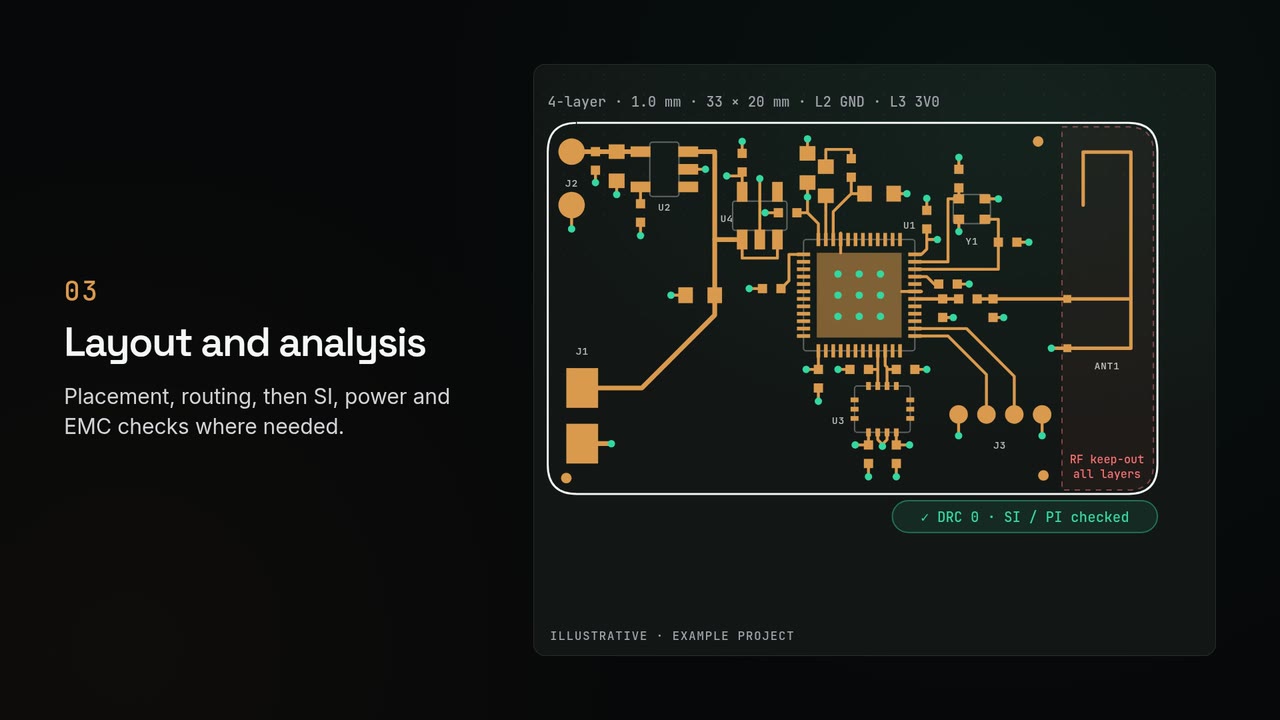
Component selection, schematic and board layout with DFM, DFT and DFA reviews.
Deliverable: Schematic, PCB layout and BOM
Inspect the assembly, check power rails and clocks, establish programming access, then exercise peripherals and interfaces.
Deliverable: Bring-up records tied to hardware and firmware revisions
Verification against the requirements, with EMC/EMI pre-compliance testing before formal certification.
Deliverable: Test evidence against project-specific exit criteria
Separate the manufacturing release from the prototype demonstration and hand over the release package.
Deliverable: Source design files, BOM and test evidence for production
Engineering notes
Embedded hardware development connects the product requirements to a buildable electronic design. Processor selection, sensing, power, interfaces and enclosure constraints need to be resolved together. The next milestone determines whether the work should produce a proof of concept, a validation prototype or a manufacturing release.
Define the bring-up sequence before the first boards arrive: inspect the assembly, check power rails and clocks, establish programming access, then exercise peripherals and communication interfaces. Record board revision, firmware version, test conditions and unresolved faults so a successful bench demonstration can be reproduced.
Choose an MCU or SoC against the actual workload, memory, interfaces and supply constraints. Estimate battery life from active, sleep and transmission duty cycles, then measure the assembled device. Radio retries, sensor settling, regulator losses and temperature can change the result; a low sleep-current specification alone does not establish product battery life.
Identify the applicable safety, EMC, radio and sector requirements before freezing the design. ISO 13485 addresses a medical-device quality management system; it is not an electrical test or blanket approval of a board. Agree the required product evidence, responsible organization and external laboratory scope with the compliance reviewer.
ISO: scope of ISO 13485Planning
Start with a non-confidential summary of your product and the milestone you need to reach next.
Describe the product's use, environment, and next development milestone. A proof of concept, a validation prototype, and a manufacturing release require different scopes and evidence.
Agree the architecture and design outputs, prototype responsibilities, verification plan, and manufacturing handoff. Identify separate laboratory, certification, tooling, and production costs before comparing proposals.
Agree confidentiality arrangements before sharing proprietary design files.
The eight factors that decide an MCU choice — performance, power, peripherals, connectivity, memory, ecosystem, supply and certification.
Flight controller vs companion computer, ESCs, LiPo, hybrid and hydrogen power, India’s Drone Rules and type certification, costs and timelines.
Proof
Industrial IoT
Steel manufacturer, India (3 plants)
Smart Agriculture
Agricultural cooperative, Maharashtra, India
Connected Fleet
Logistics and transportation company
Smart Police Wearable
State police department, India
Medical Wearable
US-based digital health startup
Digital Twin
Commercial real estate developer
Battery-Free IoT
Public infrastructure authority
Smart Urinometer
Medical device manufacturer, India
Automated Nitric Oxide Therapy System
Medical equipment manufacturer, India
AI-Powered Oxygen Therapy
Medical equipment manufacturer, India
Dexterous Robotic Hand
Indian medical-device company
Dolby Atmos Soundbar Electronics
Consumer-audio brand
Smart IV Infusion Pump
Medical-device company, India
Oral Screening Camera Probe
Medical-device client, India
Neonatal Vitals Wearable
Medical-device client, India
ToF Tank Level Monitor
Industrial client, India
Edge AI Robotics
E-commerce logistics provider
Robotic Prosthetic Arm
Prosthetics research institute
Wearable EEG Headset
Japanese neurotech startup
Wireless EMG Wearable
Fitness-wearable product company
Robotic Arm Controller Board
Robotics evaluation-board project
BLE Beacon RTLS
Asset-tracking client, Dubai, UAE
UWB Asset Tracker
Warehouse-technology company, Bangalore, India
mmWave People-Counting Sensor
Smart-building and retail client, Dubai, UAE
Hotel Call-Button System
Hospitality client, Oman
FAQ
We have extensive experience with ARM Cortex-M series (STM32, NXP LPC, Nordic nRF), ARM Cortex-A series, RISC-V architectures, ESP32/ESP8266 for IoT, Texas Instruments MSP430/C2000, Microchip PIC/AVR, and FPGA designs on AMD (Xilinx) and Altera platforms. We select the optimal processor based on your application's performance, power, and cost requirements.
Standard prototype boards up to 8 layers are fabricated and assembled through our partner PCB fabs in 48–72 hours. Complex multilayer, HDI or RF boards typically take 5–7 business days. Bring-up and functional testing follow once the boards arrive.
We design PCBs from simple 2-layer boards to complex high-density interconnect (HDI) boards up to 24 layers. Our work covers high-speed digital interfaces (DDR4/DDR5, PCIe, USB 3.x, MIPI), mixed-signal circuits, RF/antenna integration, flex and rigid-flex PCBs, and thermally optimised power electronics. We use Altium Designer, KiCad and Cadence Allegro/OrCAD.
EMC is designed in from the start: PCB stack-up design, controlled impedance routing, continuous ground reference planes, partitioned placement, EMI filtering and shielding. Pre-compliance scans at accredited partner labs come before formal certification testing, so problems are found while they are still cheap to fix. Formal testing and certification are carried out by accredited laboratories.
Yes, we specialize in ruggedized designs for industrial applications. This includes extended temperature range components (-40°C to +85°C or higher), conformal coating, vibration-resistant mounting, IP-rated enclosure designs, surge/transient protection, and compliance with industrial standards like IEC 61000 for EMC and IEC 60529 for ingress protection.
Comprehensive documentation is included with every project: schematics, PCB layout files (native + Gerber), Bill of Materials (BOM), assembly drawings, fabrication notes, test procedures, design specifications, and user manuals. All designs include Design for Manufacturing (DFM) and Design for Test (DFT) documentation for smooth production transition.
An embedded system is a specialized computer system designed to perform dedicated functions within a larger mechanical or electrical system. Unlike general-purpose computers, embedded systems are optimized for specific tasks, offering real-time performance, low power consumption, and compact form factors. Examples include automotive ECUs, medical monitoring devices, industrial controllers, and IoT sensors.
Source: Rapid Circuitry engineering team. Related terms: microcontroller, firmware, RTOS, SoC.
Weighing an external design team? Read our guide to outsourcing embedded hardware design.
Each project is quoted as a fixed-scope proposal: a statement of work with milestones, deliverables and pricing, sent within 3–5 business days of the discovery call. The price depends on the requirements, how mature the design is, technical complexity, the number of prototype iterations and the validation scope. Longer engagements can also run as a retainer or a hybrid of both. For budgeting before you contact us, our hardware development cost benchmarks and the PCB design, firmware and IoT cost guides give indicative ranges with their assumptions stated. They are planning ranges, not quotes.
It depends on the scope and on what already exists when we start. As planning ranges from our cost benchmarks: a single PCB layout takes 2–6 weeks per board and embedded firmware 4–16 weeks. A connected (IoT) product takes 3–12 months from concept to a production-ready design, and a regulated medical device 12–24 months to a 510(k) submission-ready package; from idea to mass production, a typical connected product takes 9–18 months. The proposal sets out a dated milestone plan, and you receive weekly progress updates during the project.
You do. Our contracts assign the intellectual property in the project work product (schematics, PCB design files, firmware source code and documentation) to you on payment, and we hand over the source files, not only fabrication outputs or compiled binaries. The exact terms are set out in the signed agreement for each engagement.
Yes. We sign a mutual NDA before any technical discussion of your project. Send your standard NDA or use ours; we return it signed within one business day.
Yes. We are based in Hyderabad, India, and work with product teams in India, the United States, the United Kingdom, Germany, Japan, Australia, the Middle East and other markets. Our office hours are 10:30–19:00 India Standard Time (UTC+5:30), Monday to Saturday, and we schedule design reviews across time zones, typically from US Pacific to Central European time. Japan is 3.5 hours ahead of India, so our first four hours overlap the Japanese afternoon. Prototypes and documentation ship by international courier such as DHL or FedEx. Our hardware outsourcing guide covers what to agree before an international project starts.
Yes. We prepare the manufacturing release package — fabrication and assembly drawings, the BOM with approved manufacturers, programming files and test specifications — and hand it over to the contract manufacturer (EMS) you choose. If you have not chosen one, we help you evaluate candidates through technical capability assessments and a pilot build. See manufacturing support.
No. Rapid Circuitry does not hold ISO 9001, ISO 13485 or other certificates. Our processes are aligned with ISO 9001:2015, and we design products to the requirements of the standards that apply to them — for example IEC 60601-1 and IEC 62304 for medical devices (with design documentation structured so your ISO 13485 quality system can absorb it) and IEC 61000 for EMC — and we specify IPC-A-610 workmanship classes for assembly. We prepare the product and its documentation for certification testing at accredited laboratories; the certificate or approval is issued for your product by the laboratory, notified body or regulator.
A short, non-confidential description of the product and what it must do (sensors, connectivity, on-device processing), the target production volume and unit cost, the markets and regulations it must meet (for example FDA, CE or FCC), your timeline, and what already exists: a concept, a proof of concept, schematics, PCB files or firmware. After the NDA, the next step is a 30-minute discovery call with the engineers who would work on the project, followed by the fixed-scope proposal. Send a project brief to begin.
Explore
Embedded C/C++ firmware on bare metal, an RTOS or embedded Linux: drivers, bring-up, secure boot and OTA updates.
Schematic capture and layout up to 24 layers, including HDI, rigid-flex, RF and high-speed boards, with a DFM-checked fabrication package.
Connected products from one team: sensor hardware, firmware, BLE, LoRaWAN or cellular connectivity, OTA updates and the cloud backend.