EMG Sensor Front-End
Low-Noise Myoelectric Electrode Design for Bionic-Hand Control
- Status: layout fab-ready, not yet built
- Simulated
- Input noise, vendor-model simulation
- 0.61 µVrms
- Simulated
- Mid-band gain (simulated)
- 47.7 dB
- Simulated
Core hardware
India-based PCB design services for global product teams, from schematic capture and component selection through HDI, rigid-flex, RF and high-speed multilayer layout. We deliver the design database, fabrication outputs, BOM, assembly drawings and DFM package needed for a clean manufacturing handoff.
Every project is quoted as a fixed-scope proposal within 3–5 business days of a discovery call. Discuss your product
EMG Sensor Front-End
Low-Noise Myoelectric Electrode Design for Bionic-Hand Control
Specifications
Capabilities
Precise schematic capture with hierarchical design capabilities, comprehensive part libraries, electrical rule checking (ERC), and detailed design documentation for manufacturability.
Advanced PCB layout services for boards up to 24 layers, including HDI designs with microvias, blind/buried vias, and sophisticated stackups for optimal signal integrity and power distribution.
Specialized high-speed PCB design with controlled impedance routing, length matching, differential pair handling, and simulation-driven optimization for signal integrity at frequencies up to multi-GHz.
Expert RF PCB design with proper grounding schemes, impedance matching, RF isolation techniques, and careful component placement for optimal performance in challenging wireless applications.
Proactive EMI/EMC design techniques including proper stackup design, controlled return paths, filtering, shielding, and grounding strategies that reduce the risk of failing formal EMC tests.
Comprehensive Design for Manufacturing analysis ensuring cost-effective production with optimized trace widths, proper clearances, testability features, and panelization for assembly efficiency.
Specialized thermal design including copper pours, thermal vias, component spacing optimization, and simulation-based verification to manage heat dissipation in high-power applications.
Expert design of flexible and rigid-flex PCBs with careful attention to bend radii, neutral bend axis placement, strain relief, and specialized manufacturing considerations.
Process
What a PCB design engagement hands you25 s · no sound
Confirm board outline, connector locations, layer stackup, impedance targets and fabrication limits with the intended supplier.
Deliverable: Agreed stackup, design rules and routing constraints
Hierarchical schematic capture, component selection and electrical rule checking.
Deliverable: Reviewed schematic and BOM
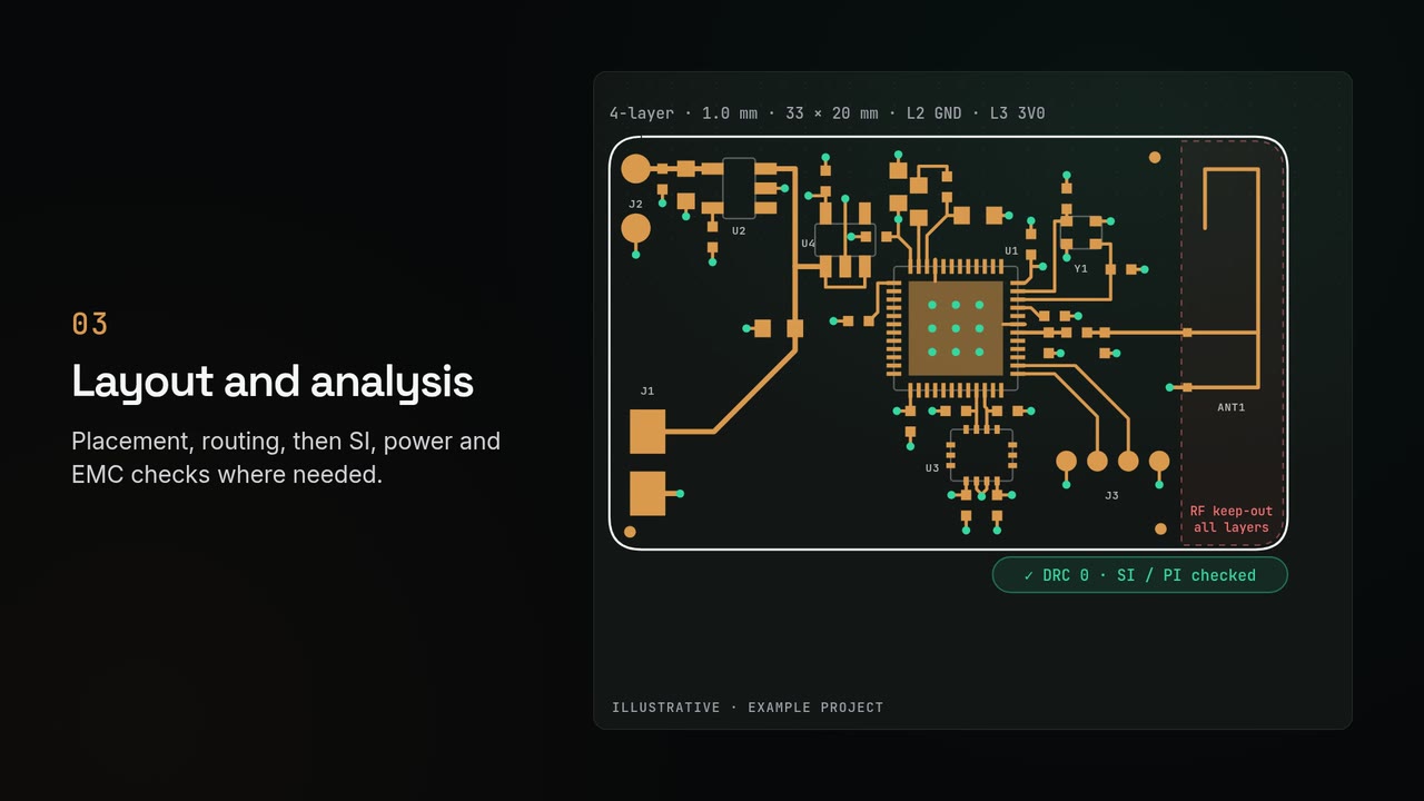
Placement and routing with interface-specific constraints; signal-integrity, power and EMC checks where the design needs them.
Deliverable: Signal integrity and design rule check reports
Resolve manufacturing queries and review the complete fabrication and assembly package on one revision.
Deliverable: Gerber/ODB++, drill files, BOM, pick-and-place data and assembly drawings
Prototype fabrication, board bring-up and validation, scoped separately from the design release.
Deliverable: Bring-up and test records against the product requirements
Engineering notes
A PCB layout is ready for release when the agreed electrical, mechanical and manufacturing checks are complete and the fabricator and assembler receive a consistent revision of the design package. Passing the CAD tool’s design-rule check is one step; it does not establish board functionality or EMC compliance.
Confirm board outline, connector locations, layer stackup, impedance targets and fabrication limits with the intended supplier. Set interface-specific routing and return-path constraints. High-speed, RF, power and rigid-flex requirements affect placement and material choices as well as trace geometry.
Keep source CAD, Gerber or ODB++ outputs, drill files, stackup notes, BOM, pick-and-place data and assembly drawings on the same revision. Review the manufacturing queries, approved substitutions, test access and unresolved exceptions before authorizing a build.
A fabrication release produces boards; bring-up and validation determine whether they meet the product requirements. For a PCB redesign or obsolete-component replacement, identify the changed interfaces, power and thermal behavior, then define the regression tests and any compliance retesting before comparing costs.
Planning
Start with a non-confidential summary of your product and the milestone you need to reach next.
A useful PCB design estimate starts with the board constraints and the files you need at handoff. Share what is known and identify the decisions that still need engineering work.
Agree the source CAD files, fabrication and assembly outputs, review reports, and responsibility for resolving manufacturing queries. Keep schematic design, layout, prototype fabrication, and board validation distinct in the quote.
Agree confidentiality arrangements before sharing proprietary design files.
Consolidated 2026 cost benchmarks for PCB design, firmware and end-to-end IoT products — by project type, complexity and region, with a transparent methodology.
Idea to mass production in six stages — feasibility, prototype, EVT, DVT, PVT and ramp — with durations, cost ranges, founder decisions, IP terms and pilot runs.
Budget the layout, check the board against manufacturing rules and review the techniques behind dense and high-speed boards.
Microvias, stackups and DFM for high-density boards.
Routing and signal-integrity practice for PCIe 6.0 layouts.
Proof
EMG Sensor Front-End
Indian medical-device company
Smart Police Wearable
State police department, India
Medical Wearable
US-based digital health startup
Multi-Connectivity Pet Tracker
European pet technology company
Smart Urinometer
Medical device manufacturer, India
Automated Nitric Oxide Therapy System
Medical equipment manufacturer, India
AI-Powered Oxygen Therapy
Medical equipment manufacturer, India
Robotic Arm Controller Board
Robotics evaluation-board project
FAQ
To begin, we need: product requirements/specifications, schematic (or component list for new designs), mechanical constraints and enclosure details, target cost and volume, regulatory/compliance requirements, and timeline expectations. We can work from rough concepts or detailed specifications depending on your project stage.
PCB cost optimization starts with panelization strategies that maximize board yield per panel, using standard materials like FR-4 and common layer counts instead of exotic stackups when possible. Avoiding unnecessarily tight tolerances on trace width, drill size, and annular ring reduces fabrication reject rates and cost. Design for manufacturability (DFM) reviews early in the layout phase can eliminate costly respins.
Our engineers are proficient in Altium Designer (primary tool), KiCad, Cadence Allegro/OrCAD and Siemens PADS, and we can import legacy EAGLE files (Autodesk retired EAGLE in June 2026). We can work with your existing design files or start from scratch. Signal integrity analysis uses HyperLynx and Ansys SIwave. Thermal analysis is performed using tools like Ansys Icepak when required.
DFM review is integral to our design process. We check component placement for automated assembly, pad/via sizes for manufacturing tolerances, trace widths/spacing for yield optimization, panelization for cost efficiency, and generate complete fabrication documentation. The aim is high manufacturing yield from the first production run, confirmed with the fab and assembler before release.
Yes, we have extensive experience with high-speed digital designs including DDR4/DDR5 memory interfaces (up to 6400 MT/s), PCIe Gen4/Gen5, USB 3.x/USB4, HDMI 2.1, and multi-gigabit Ethernet. Our designs include proper impedance control, length matching, via optimization, and signal integrity simulation to ensure reliable operation.
We design flex circuits for wearables, rigid-flex for space-constrained applications, and HDI boards with microvias and blind/buried vias. Our experience includes 0.4mm pitch BGA routing, 3mil trace/space capabilities, and designs for both standard FR4 and specialty materials like Rogers for RF applications.
Power integrity is addressed through proper power distribution network (PDN) design: adequate copper weight, strategic decoupling capacitor placement, power plane optimization, and PDN impedance analysis. For sensitive analog circuits, we implement proper star grounding, filtering, and isolation techniques to minimize noise.
Multi-layer PCB stackup design requires careful planning of layer ordering, dielectric thickness, and copper weight to achieve target impedance values and minimize signal crosstalk. Critical factors include symmetrical layer arrangements to prevent board warping, dedicated ground and power planes adjacent to high-speed signal layers, and appropriate prepreg and core material selection based on operating frequency and thermal requirements.
Effective PCB thermal management combines copper pours and thermal vias to conduct heat away from high-power components toward heat sinks or chassis ground planes. Techniques such as heavy copper layers (2 oz or greater), embedded coin inserts beneath power devices, and strategic component placement are essential. For extreme cases, metal-core PCBs or insulated metal substrates provide significantly better thermal conductivity than standard FR-4.
Controlled impedance routing is achieved by precisely calculating trace width, trace spacing, dielectric thickness, and copper weight relative to the reference ground or power plane using field-solver tools. Your PCB fabricator must maintain tight tolerances on dielectric constant and layer registration, typically verified with time-domain reflectometry (TDR) testing on impedance coupons.
HDI PCB technology uses microvias, blind and buried vias, and fine-pitch traces to pack significantly more functionality into a smaller board area, which is critical for compact consumer electronics, wearables, and medical devices. Microvias with laser-drilled diameters as small as 75 micrometers enable routing escape from fine-pitch BGA packages that would be impossible with conventional through-hole vias.
Modern PCB assembly typically uses automated solder paste stencil printing, high-speed pick-and-place machines, and reflow soldering in nitrogen-atmosphere ovens with carefully profiled thermal zones. For mixed-technology boards, selective wave soldering or pin-in-paste reflow techniques are employed after the primary SMT reflow cycle. Automated optical inspection (AOI) and X-ray inspection for hidden BGA solder joints are standard quality checks.
PCB (Printed Circuit Board) design is the process of creating the layout for electronic circuits on a board substrate. Modern PCB design involves schematic capture, component placement, trace routing, impedance control, and signal integrity analysis. PCBs range from single- and 2-layer boards to high-layer-count and high-density interconnect (HDI) designs; backplane and server boards can exceed 30 layers.
Source: Rapid Circuitry engineering team. Related terms: schematic, Gerber files, DFM, impedance control.
Each project is quoted as a fixed-scope proposal: a statement of work with milestones, deliverables and pricing, sent within 3–5 business days of the discovery call. The price depends on the requirements, how mature the design is, technical complexity, the number of prototype iterations and the validation scope. Longer engagements can also run as a retainer or a hybrid of both. For budgeting before you contact us, our hardware development cost benchmarks and the PCB design, firmware and IoT cost guides give indicative ranges with their assumptions stated. They are planning ranges, not quotes.
It depends on the scope and on what already exists when we start. As planning ranges from our cost benchmarks: a single PCB layout takes 2–6 weeks per board and embedded firmware 4–16 weeks. A connected (IoT) product takes 3–12 months from concept to a production-ready design, and a regulated medical device 12–24 months to a 510(k) submission-ready package; from idea to mass production, a typical connected product takes 9–18 months. The proposal sets out a dated milestone plan, and you receive weekly progress updates during the project.
You do. Our contracts assign the intellectual property in the project work product (schematics, PCB design files, firmware source code and documentation) to you on payment, and we hand over the source files, not only fabrication outputs or compiled binaries. The exact terms are set out in the signed agreement for each engagement.
Yes. We sign a mutual NDA before any technical discussion of your project. Send your standard NDA or use ours; we return it signed within one business day.
Yes. We are based in Hyderabad, India, and work with product teams in India, the United States, the United Kingdom, Germany, Japan, Australia, the Middle East and other markets. Our office hours are 10:30–19:00 India Standard Time (UTC+5:30), Monday to Saturday, and we schedule design reviews across time zones, typically from US Pacific to Central European time. Japan is 3.5 hours ahead of India, so our first four hours overlap the Japanese afternoon. Prototypes and documentation ship by international courier such as DHL or FedEx. Our hardware outsourcing guide covers what to agree before an international project starts.
Yes. We prepare the manufacturing release package — fabrication and assembly drawings, the BOM with approved manufacturers, programming files and test specifications — and hand it over to the contract manufacturer (EMS) you choose. If you have not chosen one, we help you evaluate candidates through technical capability assessments and a pilot build. See manufacturing support.
No. Rapid Circuitry does not hold ISO 9001, ISO 13485 or other certificates. Our processes are aligned with ISO 9001:2015, and we design products to the requirements of the standards that apply to them — for example IEC 60601-1 and IEC 62304 for medical devices (with design documentation structured so your ISO 13485 quality system can absorb it) and IEC 61000 for EMC — and we specify IPC-A-610 workmanship classes for assembly. We prepare the product and its documentation for certification testing at accredited laboratories; the certificate or approval is issued for your product by the laboratory, notified body or regulator.
A short, non-confidential description of the product and what it must do (sensors, connectivity, on-device processing), the target production volume and unit cost, the markets and regulations it must meet (for example FDA, CE or FCC), your timeline, and what already exists: a concept, a proof of concept, schematics, PCB files or firmware. After the NDA, the next step is a 30-minute discovery call with the engineers who would work on the project, followed by the fixed-scope proposal. Send a project brief to begin.
Explore
System architecture, MCU/SoC selection, schematic and PCB design, board bring-up, validation and manufacturing handoff.
Precision analog, mixed-signal and power circuits: sensor front ends, power supplies and battery management.
Antennas and RF front ends from sub-GHz to about 8 GHz, integrated and pre-scanned before radio certification.