Healthcare / Neurotech / Wearables
Wearable EEG Headset: 16-Channel Around-Ear EEG/EMG Design with Dual ADS1299 and BLE
For a Japanese neurotech startup we designed a 16-channel around-ear EEG/EMG headset: two ADS1299 front-ends, an nRF5340 BLE module and two microphones. Status: Rev C.1 design package accepted by the client as its baseline in June 2026; the hardware build was at contract stage.
Japanese neurotech startupDesign package: June 2026Rapid Circuitry hardware and firmware team
Published Last reviewed:
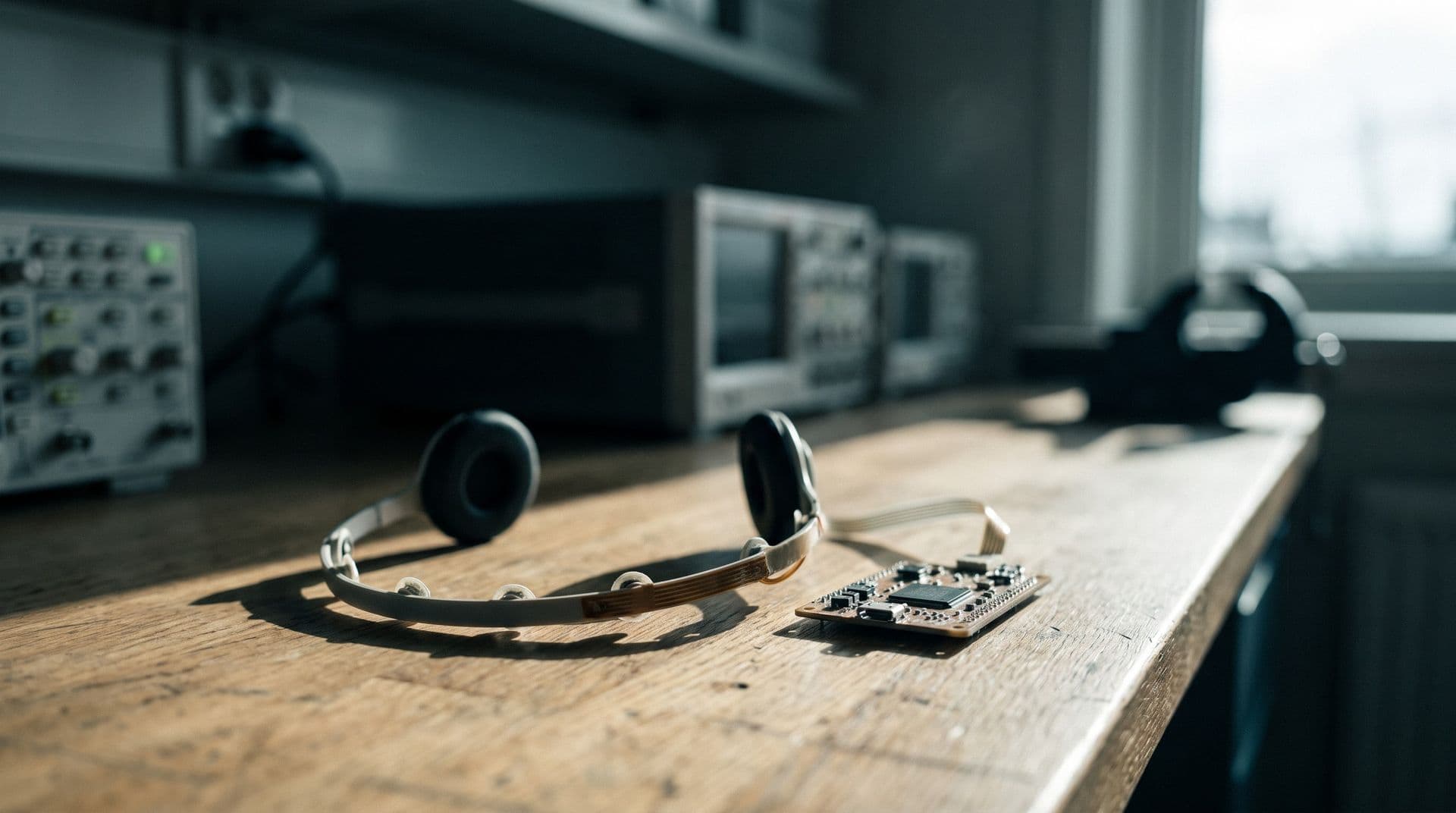 Illustrative image
The Challenge
The client needed an alpha-stage research headset that records EEG and EMG around both ears together with speech, so it can collect paired brain-signal and audio data from people at work. The electronics had to fit a 2.5 × 4.0 cm space per ear, stream everything over one Bluetooth Low Energy link, and keep microvolt-level signals clean next to a radio, a charger and microphones.
Microvolt signals in a tiny space
Each ear carries 5 EEG and 3 EMG electrodes plus shared reference and bias. The analog front-end, radio, power management and battery all had to share a 25 × 40 mm envelope per side.
Impact: Hard size limit set by the clientTwo ears, one reference
Cross-head referencing needs one shared reference and bias across both ears, but routing microvolt analog signals across the head invites noise and ground loops.
Impact: Signal integrity over a ~30 cm cableOne wireless link for everything
Sixteen 24-bit channels plus two microphone streams and status data had to fit in the goodput of a single BLE connection, with no gaps in the EEG record.
Impact: ~240–280 kbps payload (calculated)EEG and audio must line up
Speech and brain signals are analysed together, so the two streams need a common timebase that does not drift over a long recording session.
Impact: Sub-sample alignment requiredOur Solution
We produced a complete, datasheet-verified design package and took it through four architecture revisions (Rev A to Rev C.1) with the client's engineers. Each ear digitises its own electrodes locally with an ADS1299, and only digital signals plus the shared reference and bias cross between the ears.
System Architecture
Two ear boards joined by a split cable: logic and power on a flat flex cable, the microvolt reference and bias on a separate shielded, locking micro-cable.
Biosignal acquisition (per ear)
- TI ADS1299, 8 channels per ear: 5 EEG + 3 EMG
- 500 SPS, gain 24, raw data streamed (no on-device filtering)
- Cascade mode: shared SPI, separate chip-select, one shared bias amplifier
- External low-noise 2.5 V reference and dedicated 3.0 V analog LDO
- Lead-off detection, flagged rather than cleaned
Host ear: radio, audio, storage
- nRF5340 BLE module with existing FCC, IC, CE and Japan MIC radio approvals
- Two PDM MEMS microphones (one per ear) on one stereo PDM bus, Opus-encoded
- SPI-NOR flash as a retransmit buffer so dropped packets can be resent
- IMU footprint per ear with clock-in sync (firmware in V2)
- Tag-Connect SWD debug and a field-service kit
Power and interconnect
- One nPM1300 PMIC per ear; single USB-C charge port on the host ear
- Split inter-ear link: commodity 30-way FFC for logic and power
- Separate 3-core shielded, locking micro-cable for reference and bias only
- Charge and status LEDs driven by the PMICs; no always-on LED
- 6-layer, two-sided board to fit the part count
Key Parts and Design Standards
| EEG/EMG front-end | 2× TI ADS1299 |
| Wireless | nRF5340 module, BLE 2M PHY |
| Power | 2× Nordic nPM1300 PMIC |
| Analog supply | TPS7A2030 LDO + ADR4525 reference |
| Microphones | 2× PDM MEMS (stereo, one bus) |
| Sample rate | 500 SPS per channel |
| Runtime (estimate) | ~12–13 h host ear, 250 mAh cell |
| Safety framing | Designed to IEC 60601-1 style electrical-safety requirements |
| EMC plan | FCC Part 15B / EN 55032 / VCCI pre-compliance scan offered |
What We Delivered
- Feasibility assessment and component datasheet review
- Engineering design document with register initialisation and GPIO map
- Pin-accurate schematic set: pin-to-net tables for every IC and four schematic sheets
- Low-noise design guide covering grounding, supply, RF and layout
- Architecture validation report checked against primary datasheets
- Multi-discipline design review (analog, power, RF/EMC, layout, firmware)
- Rev C.1 master design document, the single source of truth
- Power analysis, BLE throughput budget and a stock-checked BOM
- Firmware and host-software scope: BLE streaming, sync and a Windows/macOS logger
- Rev C.2 engineering verdict on adding a speaker and an optional EDA channel
Key Engineering Decisions
The decisions that shaped the design, with the reason for each.
One ADS1299 per ear
Instead of routing analog signals across the head
Digitise locally; only logic crosses the cable
16 channels also exceed one chip's 8 channels
500 SPS, not 300 Hz
The requested 300 Hz is not an ADS1299 data rate
500 SPS also captures EMG better
Fallback to 250 SPS if the radio link tightens
Split the inter-ear cable
One shielded 30-way FFC of that length was not a stock part
Commodity FFC for logic, shielded micro-cable for µV nets
Every line item became a distributor-stocked part
Sync by design
ADS1299 sample counter is the master timebase
One hardware START for both ears; audio tagged with the sample index
Designed residual EEG-to-audio skew under ~50 µs
Keep the 5 V boost as a fallback
3.0 V analog supply saves area but narrows headroom
Unpopulated 5 V boost footprint on the board
Decision gated on bench tests of electrode offset
Speaker now, EDA later
Rev C.2 delta requested by the client
Populate the speaker; lay out EDA as do-not-populate
Avoids a respin without risking the schedule
How the Design Evolved
Rev A: feasibility and first architecture
Early June 2026- Confirmed the channel map: 8 signal channels per ear, which fills one ADS1299 each
- Replaced a not-recommended BLE chip with a pre-approved nRF5340 module
- Checked the BLE throughput budget and battery runtime
Rev B: client review round 1
Early June 2026- Single USB-C charge port, one power button for both ears, second I²C bus across the cable
- Flash retransmit buffer and IMU footprints added
- Validation found a GPIO collision and a far-ear charge-current limit before any layout
Rev C: client review round 2 and design-review board
Early June 2026- Added LED indication and a debug connector; moved to a 10-position electrode connector to fit the board
- Review board flagged packaging as the top risk and set 6 layers, two-sided
- Fixed schematic bugs before layout, such as two CMOS outputs tied on one ready line
Rev C.1 accepted; Rev C.2 delta assessed
Mid June 2026- Client accepted Rev C.1 as the baseline
- Assessed speaker and EDA options and recommended speaker now, EDA-ready layout
- Datasheet deep-dive caught further must-fix items before board release
Outcome and Status
The client accepted the Rev C.1 design package as its baseline for the alpha headset. At the time of writing the hardware build was at contract stage, so no bench measurements are reported here. All performance figures on this page are design calculations or estimates, not measurements.
Design accepted
Rev C.1
Accepted by the client's engineers as the baseline, June 2026
Errors caught before layout
Pre-spin
An analog LDO designed into dropout, a wrong ADC register byte, two outputs tied together and a 1.8 V / 3.3 V I/O mismatch
BLE budget
~1.4–2.5× margin
Calculated: ~240–280 kbps payload against ~400–700 kbps BLE goodput on one link
Runtime
~12–13 h
Estimate for the host ear on a 250 mAh cell, against a 4 h minimum
Technologies Used
Related Case Studies
Healthcare / Prosthetics / Biosignal
EMG Sensor Front-End: Low-Noise Myoelectric Electrode Design for Bionic-Hand Control
Consumer Electronics / Fitness Wearables