Healthcare / Prosthetics / Biosignal
EMG Sensor Front-End: Low-Noise Myoelectric Electrode Design for Bionic-Hand Control
For an Indian prosthetics company's bionic-hand programme we designed a low-noise surface-EMG electrode front-end (90–450 Hz, proportional envelope output). Status: simulation-validated, fab-ready 4-layer layout (2026); prototype not yet built.
Indian prosthetics companyDesign and simulation: June 2026Rapid Circuitry analog design team
Published Last reviewed:
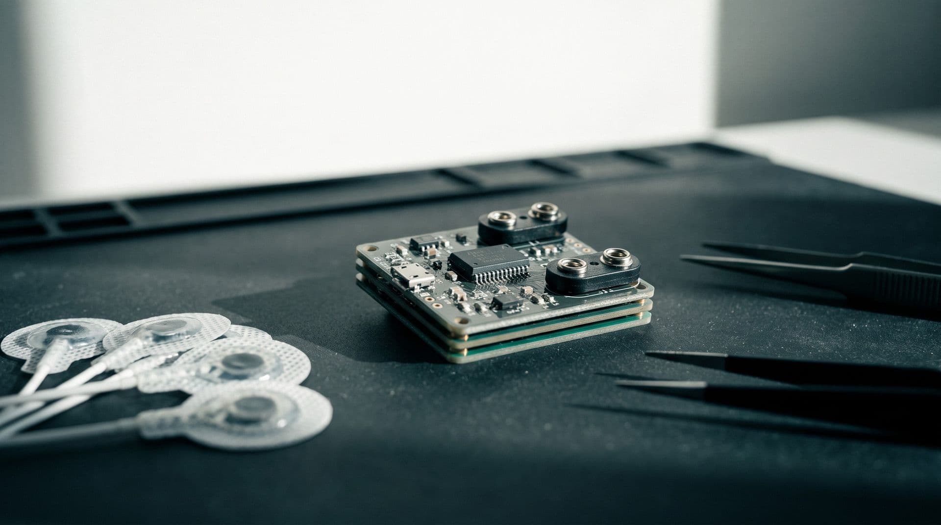 Illustrative image
The Challenge
Myoelectric hands are driven by the tiny voltages muscles produce under the skin. The client needed an electrode front-end that turns signals from about 10 µV upward into a clean, proportional control voltage, small enough to sit in a socket and robust against mains hum and electrostatic discharge.
Signals near the noise floor
Surface EMG starts at around 10 µV, so input-referred noise and amplifier choice decide whether weak contractions are usable at all.
Impact: Usable from ~10 µVMains hum and common-mode noise
The body picks up 50/60 Hz interference that can be far larger than the muscle signal. The design needed high common-mode rejection and a notch option.
Impact: 50 Hz and 60 Hz variantsSocket-sized board
The electrode had to match the size of commercial myoelectrodes, which forces a dense, 0402-heavy layout around a sensitive high-impedance input.
Impact: 27 × 18 mm envelopeProportional control output
The prosthesis controller needs a smooth envelope proportional to muscle effort, not raw EMG, delivered as a simple analog voltage.
Impact: 0–3 V envelopeOur Solution
We designed and simulated two front-end topologies in ngspice, then carried the production-style variant through a full KiCad schematic, a routed 4-layer board and a fabrication package. A structured review of placement, routing and QC before release caught a protection-circuit fault that simulation alone had missed.
System Architecture
Electrode signal to proportional control voltage on a single supply with a mid-rail reference.
Input and instrumentation amplifier
- Dual-rail BAV99 clamps on each input for ESD
- Series input resistors to the instrumentation amplifier
- AD623 instrumentation amplifier with trimmable gain
- Short, symmetric, via-free differential input pair
Filtering
- Sallen-Key high-pass at 90 Hz
- Sallen-Key low-pass at 450 Hz
- Twin-T 50 Hz notch in the discrete variant (60 Hz option)
- OPA2378 dual op-amp; MCP6004 simulated as a low-cost drop-in
Reference, supply and output
- MAX6125 2.5 V reference as the mid-rail bias
- LP2980 4.7 V LDO from the battery
- Discrete variant: precision rectifier and envelope filter to 0–3 V
- Test points and fiducials for assembly and bring-up
Key Parts and Simulated Performance
| Instrumentation amp | AD623 |
| Filter op-amp | OPA2378 (MCP6004 alternative) |
| Mid-rail reference | MAX6125, 2.5 V |
| Mid-band gain (sim) | 47.7 dB |
| Pass band (sim) | 89.8–453.9 Hz |
| Input noise (sim, vendor model) | 0.61 µVrms |
| CMRR (sim, vendor model) | 112 dB |
| Board | 4-layer, 27 × 18 mm, 38 footprints |
What We Delivered
- ngspice simulation decks for AC response, noise and transient behaviour
- Discrete zero-drift design and a production-style AD623 design
- KiCad schematic with 0 schematic-to-board parity errors
- Routed 4-layer board: 0 DRC violations, 0 unconnected nets
- Gerbers, drill files, pick-and-place and assembly drawings
- 3D STEP model of the board
- Detailed BOM with manufacturer part numbers
- Design document and simulation results summary
Key Engineering Decisions
What we chose, and why.
Fix the ESD clamps
Found in layout review, not in simulation
Single Schottky clamps to ground would conduct at the 2.5 V bias
Replaced with BAV99 dual-rail clamps
Check against vendor models
Behavioural models can mislead
Re-ran with the manufacturer's AD623 macromodel
Noise 0.61 vs 0.66 µVrms; CMRR 112 vs 100 dB
Cheap filter op-amps are fine
Filters sit after 47.7 dB of gain
MCP6004 matched OPA2378 to four decimals in simulation
Noise and CMRR are set by the input stage
Verify every pinout
Checked against datasheets and KiCad libraries
Fixed three pin and package errors before release
Reference, op-amp package and LDO pin 4
Outcome and Status
The design is simulation-validated and the board is ready for fabrication. No prototype had been built when this was written, so every performance figure on this page is a simulation result, not a bench measurement. The next step is a prototype build and bench testing on electrodes.
Input-referred noise
0.61 µVrms
Simulated with the manufacturer's AD623 model, 90–450 Hz band
Discrete zero-drift variant
0.20 µVrms
Simulated; CMRR 100 dB (+33 dB with driven right leg), 37 dB notch, envelope linearity under 0.5%
Board checks
0 / 0 / 0
DRC violations, unconnected nets and schematic parity errors
Fabrication package
Ready
Gerbers, drill, pick-and-place, assembly drawings, STEP and BOM
Technologies Used
Related Case Studies
Robotics / Prosthetics / Motor Control
Dexterous Robotic Hand: 6-DOF Motor-Control Electronics with Faulhaber Micromotors and STM32G4
Consumer Electronics / Fitness Wearables