PCIe 6.0 PCB Design Guide 2026: Routing & SI Best Practices
PCIe 6.0 PCB design pushes signal integrity engineering into territory that PCIe 5.0 layouts could mostly ignore. The jump from 32 GT/s NRZ to 64 GT/s PAM4 doubles bandwidth without doubling Nyquist frequency, but it costs roughly 9.5 dB of signal-to-noise margin and shrinks the channel insertion loss budget from 36 dB to 32 dB. For hardware teams building AI accelerators, CXL memory pools, or high-throughput storage, the layout rules that worked at Gen5 will fall over at Gen6.
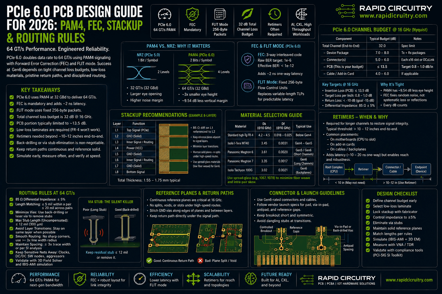
Key Takeaways
- A PCIe 6.0 channel must hit a 32 dB total insertion loss budget at 16 GHz Nyquist, with the PCB portion typically capped around 13.5 dB.
- PAM4 signaling carries 2 bits per symbol at 32 GBd, keeping fundamental frequency the same as Gen5 but cutting eye amplitude to one-third.
- Forward Error Correction is mandatory in Gen6 and adds about 2 ns of latency; FLIT mode replaces variable-length TLPs with fixed 256-byte packets.
- Standard high-Tg FR-4 is no longer adequate. Megtron 6, Tachyon 100G, and Isola I-Tera MT40 are common laminate choices for Gen6 channels.
- Retimers are typically required on server-class topologies once trace length exceeds roughly 10 to 12 inches end-to-end.
- 85 ohm differential impedance and tightly controlled return paths remain the foundation, but via stub elimination and back-drilling are non-negotiable above 32 GT/s.
What Changed in PCIe 6.0 PCB Design: PAM4 and FEC
PCIe 6.0 PCB design begins with understanding what the spec changed at the physical layer. Where Gen5 transmitted two voltage levels per unit interval (NRZ), Gen6 transmits four levels (PAM4) and carries two bits per symbol. The baud rate stays at 32 GBd, so the fundamental Nyquist frequency is still around 16 GHz. The data rate doubles to 64 GT/s per lane purely through the encoding.
From NRZ to PAM4
PAM4 looks attractive because it preserves channel frequency content, but the cost is severe. Four signal levels split the eye amplitude into three sub-eyes, each roughly one-third the height of an NRZ eye. That translates to a 9.54 dB reduction in vertical eye opening at the receiver. The board absorbs that loss through tighter passive margins and active equalization in the SerDes.
PAM4 also introduces level-dependent jitter and non-linearity that NRZ designers rarely worried about. Transmitter pre-emphasis, receiver continuous-time linear equalization (CTLE), and decision feedback equalization (DFE) all have to work harder. The PCB itself cannot fix any of this, but it can avoid making it worse with poor reference plane discipline and uncontrolled via transitions.
FEC and FLIT Mode
To compensate for the SNR loss, PCIe 6.0 makes Forward Error Correction mandatory. The FEC uses a lightweight 3-way interleaved code targeting a raw bit error rate of 1e-6 and a corrected effective error rate well below 1e-12. This is paired with FLIT (Flow Control Unit) mode, which replaces variable-length Transaction Layer Packets with fixed 256-byte FLITs. Fixed-size framing makes the FEC math tractable and bounds latency at roughly 2 ns of additional one-way delay.
For hardware teams the practical takeaway is that link reliability at Gen6 depends on a tightly engineered channel that lets the FEC deal with random noise, not systematic losses or reflections the PCB introduced.
Channel Loss Budget and Stackup
The 32 dB total channel insertion loss budget at 16 GHz is the single most important number in any Gen6 design. Everything in the channel competes for that budget: package routing, connectors, vias, and PCB traces. A typical server-class breakdown gives the PCB roughly 13.5 dB to work with, the rest going to package fanout, connectors, and cable assemblies.
Insertion Loss Targets at 16 GHz Nyquist
To stay inside that 13.5 dB PCB allowance with reasonable trace lengths, designers target insertion loss in the range of 0.8 to 1.0 dB per inch at 16 GHz on the loaded line. That is roughly half the loss per inch of a standard high-Tg FR-4 stackup, which is why material selection becomes a project-defining decision early in the schedule.
Return loss matters as much as insertion loss. Mismatches at via fields, connector launches, and component pads each contribute reflections that erode eye height after equalization. A practical target is to keep return loss below -10 dB across the band of interest, with -15 dB at critical breakpoints.
Dielectric Material Selection
Conventional FR-4 with a dissipation factor (Df) around 0.018 to 0.025 is unworkable at Gen6. The mainstream Gen6 laminates today are Panasonic Megtron 6 (Df around 0.002 at 12 GHz), Panasonic Megtron 7, Isola Tachyon 100G (Df around 0.0021 stable to 40 GHz), and Isola I-Tera MT40. The choice depends on trace length, layer count, cost ceiling, and lead time, all of which a fabricator should weigh in on before the stackup is finalized.
| Laminate | Dk (at 10 GHz) | Df (at 10 GHz) | Typical Use |
|---|---|---|---|
| Standard high-Tg FR-4 | 4.2 - 4.5 | 0.018 - 0.025 | Below PCIe Gen4 |
| Isola I-Tera MT40 | 3.45 | 0.0031 | PCIe Gen4 to Gen5 |
| Panasonic Megtron 6 | 3.61 | 0.002 | PCIe Gen5 and Gen6 short channels |
| Panasonic Megtron 7 | 3.35 | 0.0017 | PCIe Gen6 long channels |
| Isola Tachyon 100G | 3.02 | 0.0021 | PCIe Gen6 backplanes |
Spread-glass styles such as 1067 or 1078 cut the so-called fiber weave effect that causes intra-pair skew on coarser glass styles. For Gen6 the fiber weave penalty becomes significant; spread-glass or zero-glass-skew layouts are now common practice rather than an optional refinement.
Routing Rules for PCIe 6.0 PCB Design at 64 GT/s
Once the stackup is locked, the routing rules tighten on every axis: impedance, length matching, via discipline, and reference planes.
Differential Impedance and Length Matching
PCIe has standardized on 85 ohm differential impedance since Gen3 and that has not changed for Gen6. The tolerance window, however, is effectively narrower because there is less SNR headroom to absorb impedance discontinuities. A 10 percent tolerance is the typical fabrication target.
Within-pair skew should stay below roughly 2 mils on Gen6 traces. Pair-to-pair length matching is less critical for PCIe than for parallel buses, but transmit and receive trace lengths should be balanced where possible so retimer and clock recovery loops can converge predictably.
Vias, Backdrilling, and Stubs
Via stubs are reflective discontinuities and they get worse as frequency climbs. At 16 GHz a 30 mil stub on a finished panel can cost several dB of return loss. Backdrilling stub residuals to under 8 to 10 mils is standard practice at Gen6. On thick backplane builds, blind or buried vias may be preferable where the layer transition allows.
Anti-pad sizing on the via field deserves explicit attention. Oversized anti-pads can produce impedance dips well below 85 ohms; undersized anti-pads can produce capacitive humps and resonances. Closing the loop with a 3D field solver for the via transition is no longer optional at Gen6.
Reference Planes and Return Paths
Every differential pair needs a continuous reference plane along its entire route. Plane splits, voids, and changes of reference layer introduce return-path discontinuities that show up as common-mode conversion and radiated emissions. Gen6 channels tolerate none of this. Stitching capacitors and reference vias should be placed at every layer transition, and the layout should be reviewed plane by plane before signoff.
Connectors, Retimers, and Channel Topology
The 32 dB channel budget makes connector choice and retimer placement design decisions, not afterthoughts. CEM connectors, SFF-TA-1002, and OCP NIC 3.0 all have known insertion loss signatures at 16 GHz that the topology plan must absorb.
For point-to-point traces longer than about 10 to 12 inches end-to-end, including connector and cable assembly losses, a retimer becomes necessary to restore the eye. Retimers add latency, typically 5 to 20 ns, but they fully regenerate the signal, effectively breaking the channel into two shorter budgets.
A common Gen6 topology in AI accelerator chassis is host CPU to first retimer at 8 to 10 inches, retimer to riser connector, then a short trace from the riser to the accelerator. Each segment stays well inside its slice of the 32 dB budget. Redrivers are a lower-cost alternative for shorter channels but cannot fully reset the eye and are not suitable for the longest links.
For related high-speed interface tradeoffs, see Rapid Circuitry's hardware engineering resources for memory channel and stackup considerations that overlap with PCIe Gen6 design choices.
Practical Implications for Hardware Teams
Hardware teams approaching their first Gen6 board should plan for the following:
- Engage your PCB fabricator on stackup, glass style, and copper roughness before the schematic freeze. Material lead times for Gen6 laminates can be 6 to 10 weeks.
- Run pre-layout channel simulation with S-parameter models for connectors, retimers, and packages. Sign off on the loss budget before routing begins.
- Budget for backdrilling on every Gen6 layer transition by default. Treat blind and buried vias as a cost-saving option where the layer plan allows.
- Specify spread-glass or zero-skew glass styles in the fabrication notes; do not assume the default 106 or 1080 styles are acceptable.
- Order an impedance coupon and a Gen6 channel test board for first article. Calibrate insertion loss against TDR and VNA measurements on every fabrication lot.
- Plan for retimers in the BOM from day one. Schematic real estate, power, and thermal allocation for retimers are hard to retrofit.
- Validate the FEC budget end-to-end with the SerDes vendor's tools. Raw BER, corrected BER, and link training behavior should all be characterized before tape-out.
A reference design that ignores any one of these will not necessarily fail outright at Gen6, but it will fail at margin, temperature corner, or yield.
Common Questions About PCIe 6.0 PCB Design
Does PCIe 6.0 still use 85 ohm differential impedance?
Yes. The 85 ohm differential target carries forward from Gen3 through Gen6. What changes at Gen6 is the practical tolerance window: the channel has less SNR margin, so impedance variation that was acceptable at Gen5 will eat into the eye at Gen6.
Can I use standard FR-4 for short PCIe 6.0 traces?
In most cases, no. Standard high-Tg FR-4 has a dissipation factor in the 0.018 to 0.025 range, which produces 2 to 3 dB per inch of loss at 16 GHz. Even short channels eat through the PCB loss budget quickly. A purpose-built low-loss laminate such as Megtron 6 or I-Tera MT40 is the practical floor for Gen6.
How long can a PCIe 6.0 trace be without a retimer?
The answer depends on the full channel budget, but as a rough planning number, point-to-point traces above 10 to 12 inches end-to-end, inclusive of connectors and breakouts, usually require a retimer. Shorter channels can sometimes use a redriver, but for the longest links a retimer is the only option that restores the eye.
What does FLIT mode change for Gen6 board design?
FLIT mode is a protocol-layer change, not a physical-layer one, but it affects channel engineering indirectly. Fixed 256-byte FLITs make FEC and CRC math tractable at 64 GT/s. From a board-design perspective, FLIT mode means latency budgets and link training behavior look different than Gen5, and SerDes vendor tools should be configured accordingly.
How much does PAM4 hurt the noise margin?
The textbook answer is a 9.54 dB reduction in vertical eye amplitude compared to NRZ at the same baud rate, because PAM4 splits a single eye into three sub-eyes. In practice the effective hit is sometimes worse because PAM4 also amplifies non-linear effects and level-dependent jitter that NRZ designers rarely had to model.
Will PCIe 7.0 require redesigning my PCIe 6.0 stackup?
Probably yes. PCIe 7.0 doubles the baud rate to 64 GBd, pushing Nyquist toward 32 GHz and tightening the loss budget further. The laminate, copper roughness, and connector choices that work for Gen6 will be at their limits by Gen7. Designs intended to ride through both generations need to be planned for Gen7 from the start.
Working With Rapid Circuitry on PCIe 6.0 PCB Design
PCIe 6.0 PCB design is unforgiving of late decisions on stackup, retimer placement, and fabrication tolerances. Hardware teams that loop in their fab and signal-integrity partner early in the schematic phase tend to ship on time; teams that treat layout as a downstream task tend to learn about their channel budget on the test bench. If you are starting a Gen6 design and want a second set of eyes on the stackup, retimer topology, or the DFM constraints, the team at Rapid Circuitry is happy to take a look. We work on high-speed digital, RF, and mixed-signal boards across our PCB design and prototyping services. We also run pre-tape-out channel reviews for hardware teams that want a structured second opinion.
Authoritative references worth bookmarking: the PCI-SIG specification portal for the official PCIe 6.0 base spec, the IPC standards library for IPC-2581 and IPC-A-600 design rules, and the Signal Integrity Journal for current practitioner discussion of Gen6 channel design.
Need help with pcb design & prototyping?
Get a free consultation with our expert engineers. We respond within 24 hours.
Get a Free ConsultationStill researching? Read our free PCB Design Cost Guide.
Stay in the Loop
Subscribe to our newsletter for the latest updates and insights.
By subscribing, you agree to our Privacy Policy. You can unsubscribe at any time.