140 nA Sleep Current: BGM220P BLE Temperature Logger for Energy Harvesting
Introduction: How We Achieved 140–170 nA Sleep Current in a Custom BLE Temperature Logger
Building an ultra-low power IoT device sounds simple — until you realise that every nanoamp matters. The difference between a device that drains its battery in weeks and one that runs for years — or operates indefinitely from harvested energy — comes down to decisions made at every layer of the design.
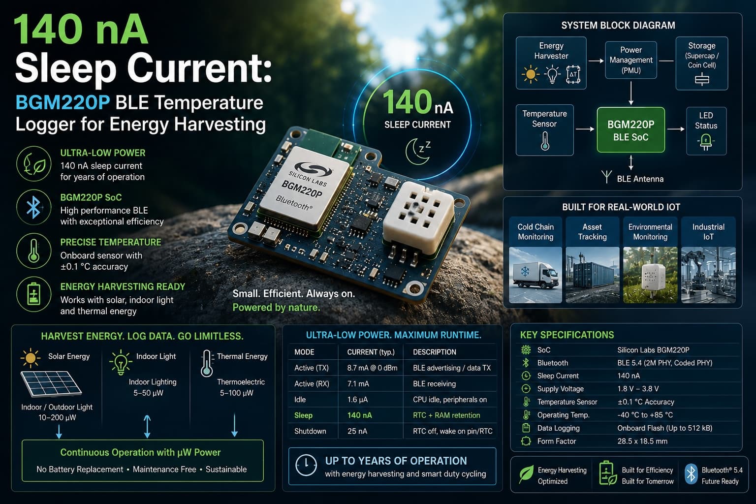
At Rapid Circuitry, we recently completed a custom BLE temperature logger built around the Silicon Labs BGM220P module. The result: a measured system sleep current of 140–170 nanoamps (nA) — the entire board, not just the chip. Here's everything we did to get there.
This blog covers:
- What Makes Ultra-Low Power Design So Challenging
- Why We Chose the BGM220P for This Application
- How Our Custom Power Circuit Hit 140–170 nA
- The Firmware Strategy That Makes It Work
- Why Sleep Current Is the Key to Energy Harvesting
If you're designing a battery-free or energy-harvesting IoT device, this is the breakdown you need.
1. The Challenge: Ultra-Low Power BLE for Energy Harvesting
Why Standard Designs Fall Short
Most off-the-shelf BLE development boards and reference designs are built for convenience, not minimum power. Pull-up resistors, debug interfaces, status LEDs, and power management ICs quietly consume 1–10 µA during sleep — already a fatal budget overrun for energy harvesting applications.
For a device powered by a harvested source — solar, thermoelectric, or RF — the system sleep current must stay in the hundreds-of-nanoamp range to be viable. This requires:
✔ Custom power delivery — every component in the power path chosen for minimum quiescent current ✔ PCB-level discipline — leakage paths identified and eliminated ✔ Firmware co-design — hardware savings are worthless if firmware keeps the device awake unnecessarily
Example:
- Standard BLE Dev Board: A typical evaluation board consumes 3–5 µA during sleep due to on-board regulators and pull-ups — already 20–35x over our target before the application even runs.
2. Why We Chose the BGM220P
A Strong Baseline for Ultra-Low Power BLE
The Silicon Labs BGM220P is a compact Bluetooth Low Energy module built on an ARM Cortex-M33 core with an integrated radio. It was our starting point for a reason:
✔ EM4 hibernate mode: sub-1.3 µA with RAM retention and RTC active ✔ Fast wake-up: wake, sample, advertise, and return to sleep in milliseconds ✔ Integrated DC-DC converter: reduces on-chip voltage regulation losses ✔ Small form factor: essential for compact wearable and industrial enclosures
The BGM220P's EM4 spec is a starting point, not the finish line. Reaching 140–170 nA at the system level required significant engineering beyond the chip itself.
Example:
- BGM220P in EM4: The SoC alone sits below 1.3 µA. Our custom power circuit brought the full board — SoC, regulator, passive network, and all — down to 140–170 nA.
3. The Custom Power Handling Circuit
A. Ultra-Low Iq Voltage Regulation
The voltage regulator is the first place most designs lose the power budget. A standard LDO can consume 1–5 µA of quiescent current on its own — exceeding the entire target budget before the SoC even enters sleep.
We selected an LDO with a quiescent current well under 500 nA to supply the BGM220P's 1.8V rail. At nanoamp-level loads, Iq is the dominant loss, not the load current itself.
✔ LDO Iq < 500 nA — keeps regulator overhead below the SoC's own sleep current ✔ 1.8V supply rail — matched to BGM220P requirements, no unnecessary voltage headroom ✔ Stable output under harvested input transients — critical for energy harvesting reliability
B. Eliminating Passive Leakage Paths
Every resistor divider and pull-up is a leakage path during sleep. A 100 kΩ pull-up on a 1.8V rail draws 18 µA continuously — catastrophic for a nanoamp budget.
✔ MΩ-range resistors used wherever voltage references were required ✔ Debug interfaces disabled in firmware and physically isolated on the PCB ✔ Non-essential peripherals power-gated via GPIO-controlled switches
C. Harvester-Compatible Input Stage
The input stage accepts energy from a range of harvesting sources — solar cells, thermoelectric generators, or RF rectifiers — without adding significant quiescent drain:
✔ Conditions harvested voltage across a wide input range ✔ Handles MPPT considerations to extract maximum available power ✔ Protects against transients and reverse polarity at the input
D. Energy Storage Sizing
A small supercapacitor buffers harvested energy for the brief active bursts during BLE advertisement. Correctly sizing this storage ensures the device completes a full wake-advertise-sleep cycle even when the harvester momentarily cannot supply enough current.
The combined result of all these measures: a system sleep current of 140–170 nA — measured across the entire board with a precision source meter on real hardware.
4. Firmware Strategy: Maximising Sleep Time
Hardware alone doesn't get you to 140 nA. The firmware must maximise the proportion of time spent in the lowest-power sleep state. Our approach:
✅ EM4 hibernate scheduling: wake only on RTC interrupt — return to EM4 immediately after ✅ Minimal active window: sensor read + BLE advertisement completes in milliseconds ✅ Non-connectable advertising: temperature broadcast directly in the advertisement payload — no connection overhead ✅ Sensor power gating: temperature sensor powered only during the measurement window via GPIO switch
By spending the vast majority of time in the 140–170 nA sleep state, the system average current remains extremely low — well within the capability of most energy harvesters.
5. Why Sleep Current Is the Key to Energy Harvesting
In a duty-cycled IoT device, sleep current dominates the power budget. If a device wakes for 20 ms every 10 seconds, it is asleep for 99.8% of its lifetime. Getting sleep current down to the nanoamp range makes previously impractical energy sources viable:
🔹 Indoor PV cells (1 cm²) generate far more than 150 nA equivalent in typical office lighting 🔹 Thermoelectric generators (TEGs) on warm surfaces can sustain the device indefinitely 🔹 Ambient RF harvesting at 2.4 GHz or 868 MHz becomes feasible at this current level 🔹 Thin-film batteries gain dramatically extended lifetimes as backup energy storage
This opens the door to truly maintenance-free, battery-free temperature sensing nodes:
✔ Cold-chain monitoring — track temperature through the entire logistics chain ✔ Industrial sensing — continuous monitoring in hard-to-reach locations ✔ Smart building infrastructure — wireless sensors with zero battery replacement ✔ Wearable patches — body-worn sensors powered by body heat or ambient energy
Example:
- Cold-Chain Logistics: A 140–170 nA logger attached to a refrigerated shipment can operate for the entire transit duration from a small harvested source — no battery swap, no maintenance, no data gaps.
Conclusion: Ultra-Low Power BLE Is a System Engineering Problem
Achieving 140–170 nA system sleep current in a functional BLE temperature logger is not just about picking the right chip. It is the result of engineering every layer of the system:
✔ Custom power circuit design — every component chosen for minimum quiescent current ✔ PCB-level leakage elimination — no passive drain paths during sleep ✔ Firmware co-design — maximise time spent in the lowest-power sleep state ✔ System-level validation — measured on real hardware with a precision source meter
The BGM220P provides an excellent foundation. But reaching nanoamp-level system sleep requires engineering the entire power delivery network — not just the SoC.
Want to Build an Ultra-Low Power IoT Device?
At Rapid Circuitry, we specialise in custom embedded hardware designed for real-world energy constraints. Whether you're targeting energy harvesting, extended battery life, or battery-free operation, our team can help.
✅ Custom PCB design optimised for ultra-low power applications ✅ Embedded firmware development for BLE, Zigbee, and proprietary wireless ✅ End-to-end prototyping from concept to validated hardware
Need help with power electronics & energy harvesting?
Get a free consultation with our expert engineers. We respond within 24 hours.
Get a Free ConsultationStill researching? Read our free How to Choose a Microcontroller (MCU).
Stay in the Loop
Subscribe to our newsletter for the latest updates and insights.
By subscribing, you agree to our Privacy Policy. You can unsubscribe at any time.