UWB PCB Design Guide 2026: Antennas, Stackup & Layout
UWB PCB design has become a near-mandatory skill for hardware teams shipping digital car keys, smart locks, and indoor positioning products in 2026. Ultra-wideband radios from ST, Qorvo, NXP, and Apple now ship in volume, and the IEEE 802.15.4ab amendment is reshaping how engineers approach antennas, stackups, and EMI. This guide covers the layout, substrate, antenna, and DFM decisions that separate a UWB design that ranges reliably at 50 meters from one that drifts.
Key Takeaways
- UWB PCB design in 2026 centers on three trade-offs: substrate loss, antenna-to-radio path control, and isolation from co-located BLE or Wi-Fi radios.
- IEEE 802.15.4z covers most current digital key and tracker products, while IEEE 802.15.4ab adds longer range, narrowband assistance, and improved non-line-of-sight performance.
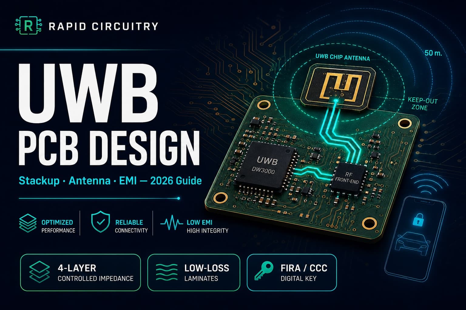
- A controlled-impedance 4-layer stackup with a continuous reference plane under the UWB antenna feed is the minimum baseline for production designs.
- Antenna placement, keep-out zones, and chassis effects dominate ranging accuracy more than firmware tuning in most field failures.
- FiRa Consortium certification and CCC Digital Key conformance are the dominant compliance paths for automotive and access-control use cases.
- Power integrity on the UWB radio rail, especially during transmit bursts, drives both ranging precision and FCC emissions margin.
Why UWB PCB Design Is a 2026 Priority
UWB has been technically available for two decades, but volume shipments are concentrated in the last three years. Smartphone makers normalized UWB in flagships from 2019 onward, and automakers followed with CCC Digital Key Release 3, which made UWB the secure ranging layer for phone-as-key systems. By early 2026, UWB is the default secure-ranging radio for digital keys and a growing share of IoT positioning.
The Standards Landscape
Two IEEE standards anchor this space today. IEEE 802.15.4z (often called "HRP UWB") is the basis of nearly every shipping consumer and automotive UWB radio. IEEE 802.15.4ab, in late-stage IEEE balloting with publication expected in 2026, extends range, adds narrowband assistance, and improves non-line-of-sight performance. New silicon families, including STMicroelectronics' ST64UWB announced in early 2026, support both standards in a single radio. For products with multi-year lifecycles, choosing a radio that can run 4ab waveforms once host firmware catches up is the safer bet.
Two Application Segments Drive Volume
The vehicle-access segment uses UWB to confirm a phone or fob is inside, outside, or near the car with centimeter-level confidence, and to thwart relay attacks against passive keyless entry. The asset-tracking and indoor-positioning segment uses UWB anchors and tags in warehouses, hospitals, and factories where GPS does not work. Both push designers toward small antennas, multi-antenna arrays, and tight integration with BLE for advertising and pairing.
Why It Matters for PCB Design
UWB transmits very short pulses spread across at least 500 MHz of bandwidth, typically in the 6.0 to 8.5 GHz range for channels 5 and 9. That bandwidth is what enables time-of-flight ranging accuracy in the 10 to 30 centimeter range, and it is also what makes the PCB design harder: substrate loss, impedance discontinuities, and antenna mismatch all eat directly into the ranging budget.
UWB PCB Design Stackup and Substrate Choices
The substrate sets the ceiling on UWB performance. A poorly chosen laminate can cost two to three decibels of link budget before the first trace is routed.
Substrate Material Trade-offs
Standard FR-4 is workable for short-range UWB modules that operate close to the antenna and tolerate a few decibels of loss, but high-volume designs targeting longer range or tight cost-per-decibel budgets often use low-loss laminates. The trade-offs map cleanly to BOM cost, manufacturability, and link budget.
| Laminate | Dk (~6.5 GHz) | Df (~6.5 GHz) | Typical UWB use | Relative cost |
|---|---|---|---|---|
| Standard FR-4 | 4.2 to 4.5 | 0.018 to 0.022 | Short-range tags, prototypes | 1.0x |
| Mid-Df FR-4 (e.g., IT-180A) | 4.0 to 4.2 | 0.012 to 0.016 | Cost-sensitive consumer | 1.2x to 1.5x |
| Hydrocarbon-ceramic (e.g., Rogers RO4350B) | 3.48 | 0.0037 | Automotive, long-range tags | 2.5x to 4x |
| PTFE-glass (e.g., Rogers RO3003) | 3.0 | 0.0010 | High-precision anchors, infrastructure | 4x to 8x |
Most consumer digital key fobs and trackers ship on mid-Df FR-4 with a low-loss laminate layer only under the antenna and front-end. This hybrid approach keeps cost manageable while protecting the most sensitive section of the board.
Stackup Recommendations
A four-layer stackup is the practical minimum for a UWB module with an integrated antenna. The standard arrangement places the antenna and the radio on the top layer, a continuous ground plane on layer two, signal and power on layer three, and a second ground plane on layer four. The layer two plane must remain continuous under both the antenna feed and the radio; splits or large via cutouts introduce impedance discontinuities that show up as ranging bias.
For products that also carry BLE or Wi-Fi, designers commonly move to six layers to give each radio its own isolated reference and routing region. A buried ground plane between the UWB and BLE sections reduces direct coupling by 8 to 12 decibels compared with a shared-plane four-layer board.
Controlled Impedance and Trace Geometry
UWB front-ends are typically 50-ohm single-ended at the antenna port. Coplanar waveguide with ground (CPWG) is the most common feed structure because it tolerates manufacturing variation better than microstrip above 5 GHz. Trace width and gap-to-ground tolerances should be specified to plus or minus 10 percent at fabrication and verified with TDR coupons on the panel. Vias in the antenna feed path should be avoided where possible; when a layer transition is unavoidable, a stitched via fence around the signal via, with stitching spacing under one-tenth of a wavelength, prevents resonances in the 6 to 9 GHz band.
Antenna Layout and Placement in UWB PCB Design
Antenna placement, not radio firmware, is the most common cause of poor ranging in UWB products in the field.
Choosing an Antenna Topology
Three antenna topologies dominate these boards. PCB-integrated patches and inverted-F antennas (IFAs) are common in low-cost trackers and key fobs because they need no extra parts. Chip antennas with characterized UWB patterns offer better repeatability across production lots, at a per-unit cost of a few cents. External antennas, connected through coaxial or board-to-board RF connectors, are used in automotive UWB anchors where placement is dictated by vehicle geometry. For most PCB-integrated designs, an IFA with a quarter-wavelength feed on a low-loss laminate is a reasonable starting point.
Keep-out Zones and Ground Plane Effects
The keep-out zone around a UWB antenna determines how predictable the radiation pattern is. A typical rule of thumb is to keep all copper, including ground fill, at least one-quarter of a wavelength away from the antenna on all sides. At 6.5 GHz, that is approximately 11.5 millimeters in free space, and roughly 6 to 7 millimeters in a microstrip on FR-4 once effective dielectric constant is taken into account. Small fobs and wearables often cannot meet that ideal; in those cases, the antenna pattern must be characterized on a representative board with the final enclosure and battery in place. Pattern shifts of 30 degrees or more between open-board prototype and final assembly are common and must be reflected in firmware lookup tables.
Multi-Antenna and Angle-of-Arrival Designs
Many UWB applications need direction information, not just distance. Angle-of-arrival (AoA) measurement requires at least two antennas separated by half a wavelength, with carefully matched feed lengths. The matching requirement is strict: at 6.5 GHz, a worst-case 10-degree AoA error budget corresponds to roughly a millimeter of feed-length mismatch, so production designs should match feeds to a fraction of a millimeter. For automotive anchors, three to four antennas per anchor are common. Anchor placement is simulated in the vehicle CAD model before PCB layout begins, because changing antenna position late is far more expensive than re-spinning a board.
Power, Clocking, and EMI Co-design for UWB
UWB radios transmit short, high-peak-current pulses. Power integrity and EMI mitigation are tightly coupled to ranging accuracy.
Power Rail Design for Burst Transmit
A typical UWB radio draws 80 to 150 milliamps during transmit bursts that last tens of microseconds. The supply rail must hold within plus or minus 3 percent during those bursts to meet the radio's specified phase noise and emissions mask. A local decoupling network with at least one bulk capacitor of 4.7 microfarads, plus 100 nanofarad and 10 nanofarad capacitors within two millimeters of the supply pins, is standard. Some radios also call for a ferrite bead on the supply rail. LDO regulators are typical, but switching regulators are acceptable if their fundamental and harmonics fall well outside the UWB band.
Clock Distribution and Phase Noise
UWB ranging accuracy depends directly on reference clock stability. Most radios specify a temperature-compensated crystal oscillator (TCXO) with frequency tolerance under plus or minus 5 parts per million. The TCXO supply must be isolated from digital noise, and the clock trace routed as a short, controlled-impedance line. In a board that hosts both UWB and an MCU running at hundreds of megahertz, MCU clock harmonics can land inside the UWB receive band. Plan MCU PLL settings during early architecture to keep third and fifth harmonics clear of the UWB channels of interest.
EMI Isolation From Other Radios
When UWB shares a board with BLE, Wi-Fi, or an LTE/5G modem, isolation planning starts at the floor plan stage. Lay out each radio's antenna and reference plane first, then route power, then digital signals last. Stitched ground fences between radio sections, RF shields placed before final EMC testing, and careful routing of antenna feed lines away from clock and digital edges are all standard practice. Authoritative guidance on controlled impedance and high-frequency layout is in IPC-2141A and IPC-2251.
External authority references hardware teams should keep in their library include the IEEE 802.15 working group page for the 4z and 4ab standards, the FiRa Consortium for interoperability and certification, and the Car Connectivity Consortium Digital Key specification for automotive deployments.
Practical Implications for Hardware Teams
For teams kicking off a UWB design in 2026, the work that pays off most is front-loaded at the architecture and stackup stage.
- Lock the UWB radio, antenna topology, and laminate before committing to the floor plan. Late changes cascade across all three.
- Plan for FiRa or CCC Digital Key conformance from the start if the product touches access control or automotive. Testing requirements influence antennas, RF, and firmware ranging behavior.
- Budget for at least one antenna characterization spin in the final enclosure. Open-board patterns rarely match production assemblies.
- Use a hybrid laminate (low-loss material only under the antenna and front-end) on cost-sensitive consumer products. Reserve full low-loss stackups for infrastructure and automotive.
- Co-design power integrity and EMI from day one. Clean transmit bursts and quiet supply rails deliver tighter ranging and lower emissions.
- Validate ranging with a tester or anchor pair before tuning firmware. Hardware issues that look like firmware bugs are common in first-pass boards.
Teams that follow this discipline typically reach FiRa-grade ranging accuracy on the second or third board revision. Teams that treat UWB as "another 2.4 GHz radio" usually take twice as many spins. The same general practices apply to neighboring radios on the same product; the Wi-Fi 7 PCB design guide and sub-GHz layout guide on this blog cover those in detail.
Common Questions About UWB PCB Design
What is the difference between IEEE 802.15.4z and 802.15.4ab for UWB PCB design?
IEEE 802.15.4z is the HRP UWB amendment used in nearly every shipping consumer and automotive UWB radio today. IEEE 802.15.4ab, in late-stage balloting with publication expected in 2026, extends usable range, adds narrowband assistance for faster acquisition, and improves non-line-of-sight performance. From a PCB perspective, 4ab does not change the frequency bands or impedance targets, but it places tighter requirements on antenna pattern stability and supply rail noise.
Can I use standard FR-4 for a UWB PCB layout?
Yes for short-range modules and prototypes, with caveats. Standard FR-4 has a dissipation factor around 0.018 to 0.022 at 6 to 8 GHz, which costs roughly one to two decibels of link budget compared with a low-loss laminate. For trackers within 10 meters of an anchor, that is acceptable. For automotive anchors, infrastructure, and any design targeting more than about 30 meters of range, a low-loss laminate under the antenna and front-end is the better choice.
How should UWB antennas be placed relative to other radios on the same PCB?
Treat UWB and 2.4 GHz radios as sharing a floor plan, not just a board. Place each antenna at the edge of the PCB with at least a quarter-wavelength of clear space (about 11 millimeters at 6.5 GHz, 30 millimeters at 2.4 GHz) from any other antenna or large metal feature. A buried ground plane between sections, plus stitched via fences, gives an additional 8 to 12 decibels of isolation.
What grounding strategy works best for a UWB radio on a 4-layer board?
Place a continuous ground plane on layer two, directly under the radio and antenna feed, with no splits or large via cutouts. Stitch vias around the antenna feed and along the RF-to-digital boundary. Avoid digital traces under the antenna keep-out zone. The radio's exposed pad must connect to the ground plane with multiple vias, typically a 3x3 or 4x4 grid sized per the radio datasheet.
How do I keep UWB EMI from coupling into BLE or Wi-Fi sections?
Most coupling between UWB and 2.4 GHz radios travels through shared ground returns and antenna near-field, not through the air. Use separate, stitched ground regions for each radio, connected at a single low-impedance bridge near the system ground reference. Route digital signals away from the UWB antenna feed, and keep MCU clock harmonics out of the UWB band. An RF shield over the UWB front-end is recommended on production-intent boards.
What certifications do UWB digital key products need?
For automotive and access-control products, the primary certifications are CCC Digital Key conformance, FiRa Consortium ranging certification, and regional radio certifications (FCC Part 15 in the US, ETSI EN 302 065 in Europe). Certification testing influences both hardware and firmware, so engaging a test lab early in the program is worth the cost.
Working With Rapid Circuitry on UWB PCB Design
UWB PCB design rewards teams that get the stackup, antenna, and power architecture right on the first revision, and punishes teams that try to fix RF problems in firmware. If your roadmap includes a digital key, asset tracker, or indoor positioning product, the time to bring a PCB design partner in is before the schematic is locked.
Rapid Circuitry's PCB design and prototyping services cover UWB stackup planning, antenna layout, EMI co-design, and DFM review for production volumes. To start a conversation about your design, reach out through the contact form and we will set up a technical review with the relevant engineers.
Need help with pcb design & prototyping?
Get a free consultation with our expert engineers. We respond within 24 hours.
Get a Free ConsultationStay in the Loop
Subscribe to our newsletter for the latest updates and insights.
By subscribing, you agree to our Privacy Policy. You can unsubscribe at any time.