Wi-Fi 7 PCB Design for IoT 2026: RF Layout Essentials
Wi-Fi 7 PCB design for IoT in 2026 is no longer a future-state discussion. With Infineon's AIROC ACW741x family and Synaptics' first AI-native Wi-Fi 7 IoT SoC reaching engineering samples this year, hardware teams now need a layout playbook that accounts for 320 MHz channels, multi-link operation, and the thermal realities of higher PHY rates in compact enclosures.
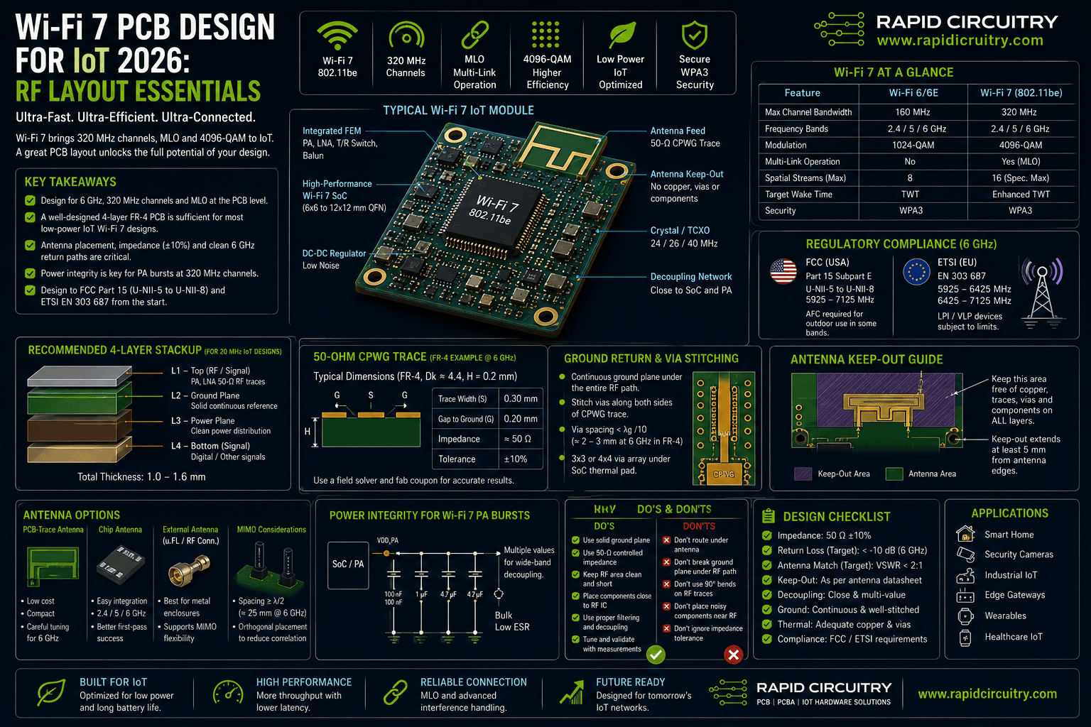
Key Takeaways
- Wi-Fi 7 PCB design for IoT must address 320 MHz channels in 6 GHz, Multi-Link Operation (MLO), and 4096-QAM at the layout level, not just at the silicon level.
- Most low-power IoT Wi-Fi 7 designs can stay on 4-layer FR-4 stackups if the 50-ohm RF trace, ground return, and antenna keep-out are handled correctly.
- Antenna placement, impedance matching to within plus or minus 10%, and clean 6 GHz return paths are the three most common failure points in first-pass Wi-Fi 7 prototypes.
- Power integrity for the PA bursts at 320 MHz channels requires careful decoupling and low-ESR bulk capacitance close to the SoC.
- FCC Part 15 Subpart E (U-NII-5 through U-NII-8) and ETSI EN 303 687 govern 6 GHz emissions and need to be designed in from the schematic stage.
Why Wi-Fi 7 Matters for IoT Hardware in 2026
Wi-Fi 7, formally IEEE 802.11be, is rolling out across IoT silicon this year in two distinct flavors. The full-bandwidth variant targets gateways, cameras, and AR/VR endpoints with 320 MHz channels, 4096-QAM, and up to 16 spatial streams in the spec maximum (though typical IoT silicon ships 2x2). The 20 MHz IoT variant, recently introduced by Infineon, keeps the lower bandwidth from Wi-Fi 6 but adds MLO, Target Wake Time enhancements, and improved coexistence with Bluetooth LE 6.0 and 802.15.4 Thread. Both variants share the same Wi-Fi 7 PCB design constraints around RF integrity, antenna isolation, and 6 GHz operation.
What changes versus Wi-Fi 6 at the board level
The jump from Wi-Fi 6/6E to Wi-Fi 7 introduces three layout-relevant changes. First, the 6 GHz band is now in scope for nearly every Wi-Fi 7 IoT SoC, which doubles the highest operating frequency the antenna feedline must support cleanly. Second, MLO requires two or three radios operating simultaneously, which forces tighter isolation between RF sections. Third, 4096-QAM has very low EVM margin, so phase noise from the reference oscillator and ground bounce on the PA supply matter more than they did at 1024-QAM.
Where Wi-Fi 7 lands in your bill of materials
Most Wi-Fi 7 IoT chipsets in 2026 are highly integrated single-die solutions with on-chip PA, LNA, T/R switch, and balun. That integration matters for PCB design because it reduces the discrete RF component count, but it also concentrates heat near the antenna feed. Expect to see QFN packages between 6x6 mm and 12x12 mm with thermal pads that need a deliberate copper pour and via stitching strategy.
Wi-Fi 7 PCB Design: RF Layout Fundamentals
The RF section of a Wi-Fi 7 design is the part that fails first when corners are cut. The fundamentals have not changed, but the tolerances have tightened with the move to 6 GHz.
Stackup choices for 6 GHz operation
For 20 MHz Wi-Fi 7 IoT modules with integrated front ends, a well-controlled 4-layer FR-4 stackup is usually enough. The classic arrangement is signal on layer 1, ground on layer 2, power on layer 3, and signal on layer 4. The 50-ohm RF trace runs on layer 1 as a coplanar waveguide with ground (CPWG), referenced to the solid ground on layer 2. For 320 MHz Wi-Fi 7 with multiple spatial streams or external front ends, you may need to move to low-loss laminate such as Panasonic Megtron 6, Rogers RO4350B, or Isola I-Tera MT40 to keep dielectric loss within the link budget.
50-ohm trace geometry at 6 GHz
CPWG is the practical choice for Wi-Fi 7 RF traces because it confines the field and reduces sensitivity to nearby copper. With FR-4 at Dk around 4.4 and a 0.2 mm prepreg between L1 and L2, a 0.30 mm trace with 0.20 mm ground clearance typically lands near 50 ohms. The exact dimensions depend on your laminate, so use a field solver such as Saturn PCB Toolkit or your fab's calculator, and ask your fab for impedance-controlled fabrication with a measured coupon.
Ground return integrity
A continuous reference plane under the entire RF path is non-negotiable. Any split in the L2 ground beneath the 6 GHz trace creates an impedance discontinuity that shows up as return loss degradation in S11. Stitch ground vias along both edges of the CPWG trace at a spacing well under one-tenth of the guided wavelength at 6 GHz, which in FR-4 works out to roughly 2 mm to 3 mm. The same rule applies under the SoC thermal pad, where a 3x3 or 4x4 via array bonds the package ground to L2.
Antenna Placement and Impedance Control
Antenna design is where most Wi-Fi 7 IoT prototypes lose their margin. The good news is that the rules are well understood; the bad news is that they get violated under mechanical pressure to shrink enclosures.
PCB-trace antennas versus chip antennas
For low-cost 20 MHz Wi-Fi 7 IoT designs, a PCB-trace antenna such as an inverted-F (IFA) or meandered monopole remains viable in both 2.4 GHz and 5 GHz bands, but 6 GHz support tightens the tolerance budget significantly. Chip antennas from Pulse, Ignion, or Johanson with published 2.4/5/6 GHz tuning are often the safer choice for a first board. External U.FL or RF connectors are appropriate when the device sits inside a metal enclosure or needs MIMO with spatial separation.
Keep-out and ground reference
Every antenna vendor publishes a keep-out region under and around the antenna footprint. Treat that as a hard constraint. The keep-out must be free of copper on all layers, including ground, with no traces, vias, or components inside the boundary. The ground plane should end cleanly at the keep-out edge, with no slots or fingers protruding into the antenna region. For PCB-trace antennas, the ground extension behind the antenna becomes the radiator's counterpoise and must be sized to the vendor's reference layout.
Matching network and S11 targets
Plan for a pi-network with three 0402 placements between the SoC RF output and the antenna feed. Most designs do not need all three components populated, but the footprints give you tuning headroom after the first S-parameter sweep on a VNA. The practical target is S11 better than -10 dB across 2.4 GHz, 5 GHz, and 6 GHz, with -7 dB acceptable at the band edges if certification testing shows TIS and TRP within spec.
Power Delivery and Thermal Considerations
A Wi-Fi 7 SoC operating at 320 MHz channels and 4096-QAM draws significant current during TX bursts. The PDN must handle those transients without sagging or ringing, and the package must shed the heat that the PA generates.
PA supply decoupling and bulk capacitance
Place a 0.1 uF 0402 ceramic on every SoC supply pin within 1 mm of the pin, with the return via inside the pad. Add a 1 uF or 4.7 uF 0603 reservoir per supply rail within 5 mm. The PA rail benefits from an additional 10 uF to 22 uF low-ESR ceramic or polymer bulk capacitor on the same plane. Avoid placing decoupling on the bottom layer if it forces the return current to detour around vias.
Thermal pad design and via stitching
The SoC thermal pad on the bottom of a QFN must be connected to the inner ground plane with a via array. A 4x4 grid of 0.25 mm vias with 0.5 mm pitch is a reasonable starting point for a 7x7 mm package. Tent the vias on the top side or use via-in-pad with epoxy fill if the assembly process supports it, to avoid solder wicking during reflow. Confirm the recommended pattern with the SoC datasheet, as some vendors specify a tighter grid.
Comparison of Wi-Fi 7 IoT design choices
| Design Choice | 20 MHz Wi-Fi 7 IoT | Full Wi-Fi 7 (160/320 MHz) |
|---|---|---|
| Typical stackup | 4-layer FR-4 | 4 to 8 layers, low-loss core |
| Antenna type | PCB trace or chip | Chip array or external MIMO |
| Channel bandwidth | 20 MHz | Up to 320 MHz |
| Modulation | Up to 4096-QAM | Up to 4096-QAM |
| Power draw (TX peak) | Low (sub-500 mW typical) | Moderate to high |
| Target applications | Sensors, smart home, BLE coexistence | Gateways, cameras, AR/VR |
| Certification complexity | Moderate | Higher (6 GHz AFC, MLO testing) |
EMC, Certification, and DFM
Designing for compliance and manufacturability from day one shortens the path from prototype to volume.
6 GHz regulatory landscape
The 6 GHz band in the United States is governed by FCC Part 15 Subpart E and is split into U-NII-5 through U-NII-8 sub-bands. Standard-power operation in U-NII-5 and U-NII-7 requires Automated Frequency Coordination (AFC), while Low Power Indoor (LPI) operation does not. ETSI EN 303 687 covers the equivalent European requirements. Identify the operating profile early because it changes both the antenna gain budget and the firmware certification path.
Pre-compliance EMI strategy
Add ferrite bead footprints on every digital interface entering the SoC, especially USB, MIPI, and high-speed SPI links that can radiate into the 5 GHz and 6 GHz bands. Keep the crystal or TCXO reference oscillator inside its own grounded copper pour and route the load capacitor traces as short as physically possible. Plan a guard-band cutout between the digital section and the RF section if your enclosure does not provide RF shielding.
Design for manufacturability checks
Use 0402 components on the RF path for repeatable solder profiles, and avoid 0201 unless your CM has demonstrated capability at scale. Keep RF reference designators on the silkscreen but locate them outside the antenna keep-out. Specify the controlled-impedance coupon on the panel so the fab can certify the 50-ohm trace dimensions on every build.
Practical Implications for Hardware Teams
The shift to Wi-Fi 7 affects schedule, BOM, and process. Teams that adapt early avoid the late-stage surprises that delayed many Wi-Fi 6E launches.
- Lock the stackup with your fab before the first layout pass, because Wi-Fi 7 trace impedance and dielectric loss budgets do not tolerate substitution at the last minute.
- Choose your antenna vendor and reference design before placing the SoC, since the antenna keep-out drives the floorplan more than any other constraint.
- Budget for a VNA-based S-parameter sweep on the first prototype, with calibrated probes at the antenna feed and at the SoC output pad.
- Plan for two layout spins: one for first-pass RF tuning and one for EMC and thermal hardening after pre-compliance testing.
- Align the firmware certification path with the regulatory profile from the start, since LPI and standard-power 6 GHz operation have different test scopes.
- Engage your contract manufacturer on stencil design and reflow profile for the QFN thermal pad before pilot production, not after.
Common Questions About Wi-Fi 7 PCB Design
Do I need a 6-layer PCB for a Wi-Fi 7 IoT product?
Not usually. A well-executed 4-layer FR-4 stackup is sufficient for most 20 MHz Wi-Fi 7 IoT modules with an integrated front end. Move to 6 or 8 layers when you need internal power and ground planes for high-current digital sections, when you have external PA or LNA components, or when MLO with three radios forces dedicated routing layers.
What antenna impedance should I target for Wi-Fi 7?
A 50-ohm system impedance is standard, and you want S11 better than -10 dB across the operating bands. The matching network should be designed as a three-component pi-network footprint, with the final values determined after measuring the antenna in your enclosure on a VNA.
How is Multi-Link Operation different from MIMO in PCB terms?
MIMO uses multiple antennas on the same band for spatial multiplexing, while MLO uses radios on different bands simultaneously, typically 5 GHz and 6 GHz together. In layout terms, MLO requires high isolation between the band-specific antenna feeds, similar to Wi-Fi 6E dual-band design but with tighter isolation targets due to the higher PHY rates.
Can I use a chip antenna at 6 GHz?
Yes. Several vendors now ship tri-band chip antennas qualified for 2.4 GHz, 5 GHz, and 6 GHz operation. The trade-off versus a PCB-trace antenna is BOM cost and procurement risk, balanced against tighter performance tolerances and a smaller PCB footprint.
What is AFC and does my IoT device need it?
Automated Frequency Coordination is a database-driven mechanism that lets Wi-Fi 7 devices operate at standard power in U-NII-5 and U-NII-7 without interfering with incumbent licensed users. Battery-powered indoor IoT devices typically use Low Power Indoor mode and do not need AFC, while gateways and outdoor equipment may require it.
How early should I bring in my contract manufacturer for a Wi-Fi 7 design?
As early as the stackup decision. Wi-Fi 7 designs benefit from a CM review on impedance control, controlled-depth drilling if used, and QFN reflow profile before the schematic is frozen. Late-stage CM input on a Wi-Fi 7 board is one of the most common causes of yield issues in pilot runs.
Working With Rapid Circuitry on Wi-Fi 7 PCB Design
Wi-Fi 7 PCB design works best when RF, power, and thermal are treated as a single coupled problem from the first schematic review. We have helped customers take Wi-Fi 6 and Wi-Fi 6E products from concept to certified production, and the Wi-Fi 7 transition applies the same approach with tighter tolerances and a sharper focus on 6 GHz. If you are scoping a new IoT product, evaluating a Wi-Fi 7 module versus a chip-down approach, or planning a re-spin to upgrade an existing Wi-Fi 6 design, contact our hardware team and we can review the stackup, antenna, and certification path with you. You can also see how we approached related challenges in our HDI PCB design guide and our Matter and Thread hardware design guide, both of which share constraints with Wi-Fi 7 IoT designs. For deeper standards reading, the IEEE 802.11be specification and the Wi-Fi Alliance Wi-Fi 7 program are the authoritative starting points.
Need help with iot & wireless communication?
Get a free consultation with our expert engineers. We respond within 24 hours.
Get a Free ConsultationStay in the Loop
Subscribe to our newsletter for the latest updates and insights.
By subscribing, you agree to our Privacy Policy. You can unsubscribe at any time.