HDI PCB Design Guide 2026: Microvias, Stackups & DFM
HDI PCB design has moved from "nice to have" on flagship phones to a routine requirement on industrial IoT, edge AI, and wearable boards shipping in 2026. Tighter component pitches, denser BGAs from on-device AI accelerators, and shrinking enclosures have pushed mainstream hardware into microvia territory. This guide walks through HDI PCB design from the angles that matter most in practice: microvia classes, stackup choices, and DFM rules engineering teams need to specify HDI builds without surprises at the fab.
Key Takeaways
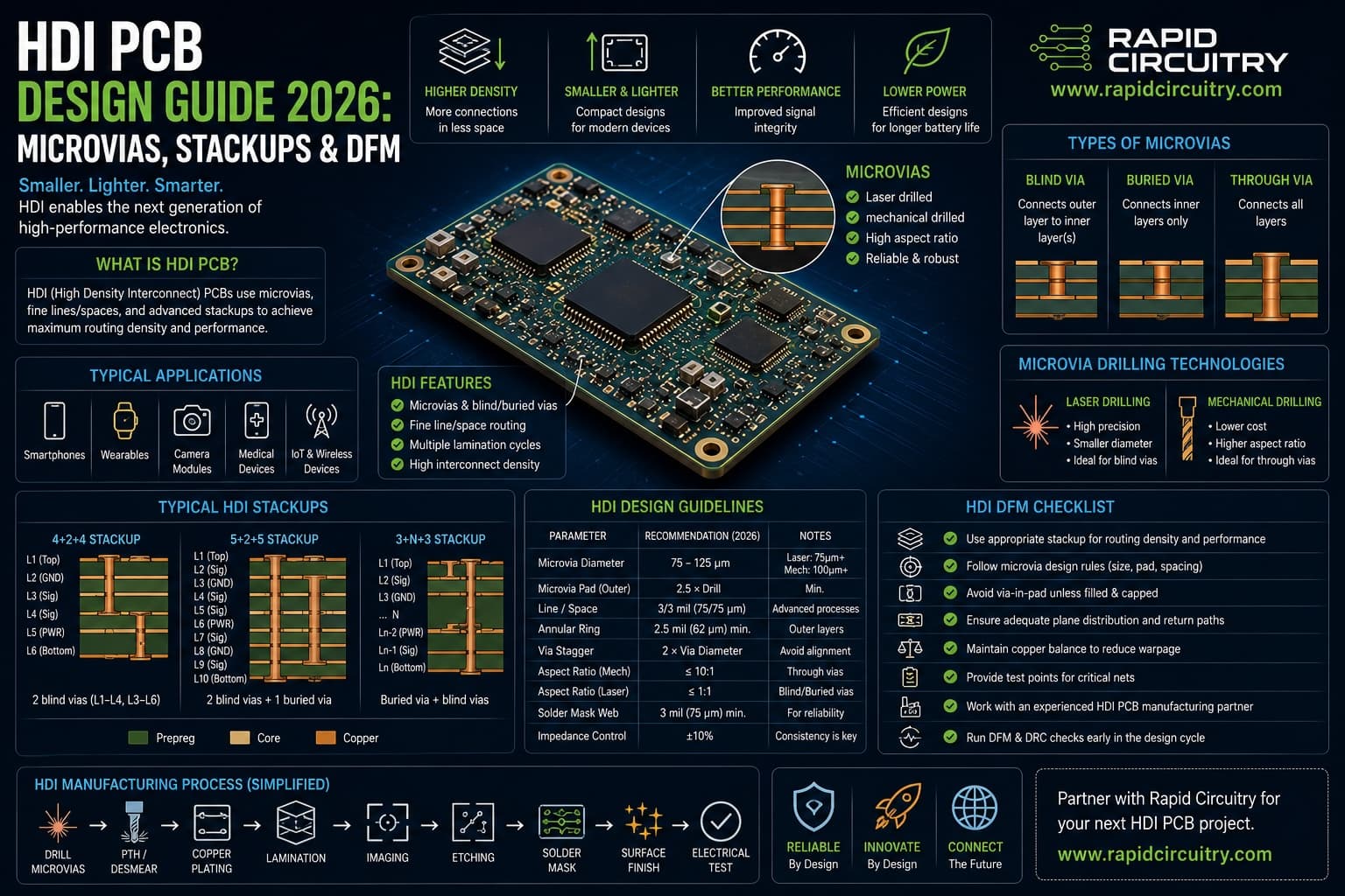
- HDI PCB design is defined by microvias (≤150 µm finished diameter) and finer trace/space than conventional PCBs, per IPC-2226.
- Microvia aspect ratio should stay at or below 1:1 (depth:diameter) to keep plating reliable; stacked microvias add reliability risk and need explicit qualification.
- Type I, II, and III HDI structures trade cost for routing density; most IoT and edge AI boards land on Type I or Type II.
- Via-in-pad with copper-fill is the practical way to fan out 0.4 mm pitch BGAs without sacrificing signal integrity.
- DFM headaches usually come from sequential lamination cycles, copper-fill flatness, and laser-drill registration — talk to the fab before you finalize the stackup.
- HDI does not automatically mean better signal integrity; it lets you shorten return paths, but the stackup and reference planes still do the work.
What HDI PCB Design Means in 2026
HDI stands for High-Density Interconnect. The IPC-2226 standard defines an HDI PCB as one using microvias, fine lines (typically below 100 µm trace/space), and high pad density. In modern HDI PCB design, the practical trigger is component pitch. Once a BGA drops below 0.5 mm pitch, conventional through-hole vias cannot fan out without via-starvation or impossible escape routing. That is where microvias and HDI stackups become unavoidable.
Three forces have pushed HDI from premium consumer electronics into mainstream hardware in 2026. On-device AI accelerators are arriving in 0.35 mm and 0.4 mm pitch BGAs that simply cannot be escaped from a standard 6-layer board. Industrial IoT gateways are shrinking to fit DIN-rail and sensor-node enclosures, forcing layer counts up and via diameters down. And memory packages — particularly LPDDR5 and emerging LPDDR5X variants — ship in fine-pitch FBGAs whose ball maps assume HDI escape patterns.
The result is that HDI is no longer the exotic option. For many edge AI and connected industrial boards, it is the only path that closes layout in a reasonable layer count.
How HDI PCB Design Differs From Conventional PCB Design
A conventional 6- or 8-layer PCB uses through-hole vias drilled mechanically across the full stack. Trace/space is typically 4 mil / 4 mil (≈100 µm). Annular rings, drill tolerances, and via aspect ratios drive how dense you can pack components.
HDI PCB design replaces some or all of those through-holes with laser-drilled microvias that span only one or two dielectric layers at a time. This frees routing channels under BGAs, shrinks pad-to-via spacing, and allows trace/space down to 2 mil / 2 mil (≈50 µm) or finer on advanced builds. The trade-off is sequential lamination — each microvia layer adds a press cycle, and each cycle adds cost, registration risk, and lead time.
Microvia Construction in HDI PCB Design: Types, Aspect Ratios, and Failure Modes
A microvia is laser-drilled, typically with a UV or CO2 laser, and copper-plated to form an interconnect between adjacent layers. In HDI PCB design, IPC-2226 and the related IPC-6012 performance specs set the boundaries.
Microvia Geometry and Aspect Ratio
The dominant reliability constraint is aspect ratio, defined as the depth-to-diameter ratio of the drilled hole. For a single-level microvia, IPC guidance treats 0.75:1 as the preferred aspect ratio for plating uniformity, with 1:1 as the absolute maximum. A 100 µm diameter microvia, for example, should connect layers separated by no more than 100 µm of dielectric.
Pushing aspect ratio higher tends to produce voids in the plated copper and weak interface bonds at the target pad. Those defects do not always show up at electrical test; they fail later under thermal cycling. IPC-TM-650 method 2.6.7.2 (thermal shock and continuity for printed boards) and the microvia-specific D-coupon protocol described in IPC-9252 are the standard ways to qualify a microvia process before shipping volume.
Stacked vs. Staggered Microvias
When you need to span more than one dielectric layer, you have two choices. Staggered microvias are offset on each layer, with a short trace connecting them. Stacked microvias sit directly on top of each other with a copper-filled pad between them.
Staggered designs are easier and more forgiving — each microvia is independent. Stacked designs save board area and improve signal integrity for high-speed nets, but every interface is a reliability stress concentrator. IPC-6012 Class 3 boards (medical, automotive, aerospace), and the addenda IPC-6012EM (medical) and IPC-6012EA (automotive), impose stricter qualification on stacked structures, including additional thermal cycle counts and cross-section inspection.
For most IoT and consumer-edge designs, staggered microvias are the safer default in HDI PCB design. Move to stacked only when the routing or signal integrity case is clear.
Common Microvia Failure Modes
Three failure modes dominate field returns on poorly executed HDI builds. First, target pad separation, where the plated copper detaches from the underlying pad after thermal cycling. Second, plating voids inside the via barrel, usually from poor desmear or aggressive aspect ratio. Third, copper crack propagation at the knee of the via, especially in stacked structures under repeated reflow or operating thermal swings.
The fab process windows that prevent these are well understood, but only if your design respects the geometric limits. Aspect ratio, dielectric thickness, and pad-to-via offset are the levers in the designer's hands.
HDI PCB Design Stackup Strategies for IoT and Edge AI Boards
IPC-2226 classifies HDI boards by structure. The structure class you specify in HDI PCB design determines layer count, lamination cycles, and cost.
HDI Build-Up Types Compared
The cost ranges below reflect typical 2026 fab pricing observed in the industry; actual quotes vary with volume, fab, and material choices.
| HDI Type | Structure | Typical Layer Count | Lamination Cycles | Relative Cost | Best For |
|---|---|---|---|---|---|
| Type I | One microvia layer on each side of a cored board | 4–8 | 1 sequential | 1.3–1.6x standard | Wearables, simple IoT nodes |
| Type II | Type I plus buried vias in the core | 6–10 | 2 sequential | 1.6–2.0x standard | Industrial IoT, edge AI starter boards |
| Type III | Two or more microvia layers on each side | 8–14 | 3+ sequential | 2.0–3.5x standard | Smartphones, dense edge AI, fine-pitch BGAs |
| ELIC (any-layer HDI) | Microvias on every layer; no through-holes | 10+ | Multiple | 3.0x+ standard | Flagship mobile, advanced AI accelerators |
Most industrial IoT and embedded edge AI boards land on Type I or Type II HDI PCB design. Type III and ELIC remain the territory of high-volume mobile and bleeding-edge accelerator hardware.
Picking a Stackup for a 0.4 mm BGA
A 0.4 mm pitch BGA cannot be escaped with through-hole vias alone — there is not enough pad-to-pad clearance. The standard fan-out pattern uses via-in-pad microvias on the BGA layer and a second microvia on the layer below to drop signals into routing channels.
For a 12 mm × 12 mm BGA with roughly 600 balls, this typically means a Type II or Type III build with at least 8 routable layers. An LPDDR5 memory interface with 32-bit width adds another 60–80 high-speed nets that need controlled-impedance reference planes, which pushes layer count further.
Reference Planes and Signal Integrity
A common mistake is to assume HDI automatically improves signal integrity. It does not. What HDI gives you is the freedom to put high-speed traces close to clean reference planes by shortening vertical transitions. If your stackup still has signal layers referenced against split planes or against signal layers, HDI will not save you.
The discipline is the same as on a conventional board: every high-speed signal layer must reference a continuous plane on at least one adjacent layer. HDI just gives you more freedom to arrange layers without exploding the layer count.
DFM Rules and IPC-2226 Compliance for HDI PCB Design
Design-for-manufacturing in HDI PCB design is where most teams lose time. The fab's process window and your design rules need to agree before you tape out.
Microvia Geometric Limits
Common 2026 fab capabilities for mainstream HDI run roughly as follows. Laser-drilled microvia diameter is typically 75–150 µm, with 100 µm as the volume-friendly default. Capture-pad diameter is 200–250 µm for a 100 µm microvia. Dielectric thickness between microvia layers is 50–100 µm, matched to the microvia diameter. Trace and space on outer layers run 50–75 µm; inner layers can hold 50/50 µm but require closer fab coordination.
These numbers are not standards — they are what most established HDI fabs offer at production volume. Advanced fabs go finer, and consumer mobile fabs run sub-50 µm features at scale, but cost and lead time scale with capability.
Via-in-Pad and Copper Fill
Via-in-pad is essential for fine-pitch BGAs but introduces a new failure mode. If the via barrel is not filled, solder paste during assembly wicks down the via, leaving voids in the BGA joint. The standard fix is electrolytic copper fill — the plating step is extended until the via is fully closed and a flat copper cap covers the pad.
Copper fill is well-controlled on Type II and Type III HDI. Make sure your fab knows you require filled microvias on every BGA pad and that you call it out on the fab notes. IPC-4761 defines the via protection types you should reference: Type VI is "filled and covered," and Type VII is "filled and capped" — Type VII is the spec for via-in-pad applications. Using IPC-4761 language on the drawing prevents ambiguity.
Sequential Lamination and Registration
Each microvia layer requires its own lamination press cycle. Two microvia levels per side mean three to four total press cycles. Each cycle introduces dimensional drift in the copper and dielectric, which the fab compensates for with scaling factors. The risk is registration loss between layers — pads and microvias on layer 4 may not line up perfectly with the structures laid down on layer 3.
Practical mitigation: keep capture pads generous (don't push to absolute minimum), keep microvia structures away from board edges where dimensional drift is largest, and resist the temptation to specify maximum-density features in every region of the board. HDI is most reliable when the dense regions are local to the components that need them.
Practical Implications for Hardware Teams
- Decide on HDI PCB design vs. conventional in the schematic phase, not in layout. Component selection drives the answer.
- Get a stackup proposal from your fab before placing parts. Your fab knows their press limits and dielectric inventory better than any reference table.
- For BGA pitches at or below 0.5 mm, plan on via-in-pad with electrolytic copper fill. Specify it in the fab notes using IPC-4761 Type VII (filled and capped) language.
- Treat aspect ratio as a hard constraint. A microvia drilled deeper than its diameter will eventually fail in thermal cycling, even if it passes electrical test.
- For Class 3 applications (medical, automotive, aerospace), require thermal-cycle qualification per IPC-TM-650 method 2.6.7.2 and the IPC-9252 D-coupon protocol before locking the build.
- Keep dense HDI regions local. The cost of an HDI board scales with the worst-case feature, not the average.
- Document microvia structures (stacked vs. staggered) on the fab drawing. Don't rely on the fab to infer it from the layer view.
Common Questions About HDI PCB Design
What is the smallest microvia size achievable in production in 2026?
Mainstream HDI fabs reliably produce 75–100 µm microvias at volume. Advanced mobile fabs go below 50 µm, but at higher cost and tighter design rule constraints. For a first HDI design, 100 µm is the safe default.
When should I move from a conventional PCB to HDI PCB design?
The straight answer is: when component pitch forces it. A 0.5 mm BGA can sometimes escape on a well-planned 8-layer conventional board. A 0.4 mm BGA almost always needs HDI PCB design. Above 0.5 mm pitch, HDI rarely pays off unless you have severe layer-count or board-area constraints.
How much more expensive is HDI PCB design compared to a conventional PCB?
Per the cost ranges in the comparison table above, Type I HDI PCB design runs roughly 1.3–1.6x conventional, Type II runs 1.6–2.0x, and Type III runs 2.0–3.5x. Volume narrows the gap; prototype quantities can see larger multipliers.
Can microvias be stacked on top of each other?
Yes, but stacked microvias add reliability risk because every interface is a stress concentrator. For Class 2 commercial boards, stacked is acceptable if the fab process is qualified. For Class 3 (medical, automotive, aerospace), staggered is preferred unless you have a strong routing reason and a qualification plan.
Does HDI PCB design improve signal integrity for high-speed IoT and edge AI nets?
Indirectly. HDI PCB design lets you arrange reference planes closer to high-speed signal layers and shortens vertical transitions, both of which help signal integrity. But a poorly stacked HDI board will still have signal integrity problems. The stackup discipline matters more than the via technology.
What is the difference between HDI Type I, Type II, and Type III?
Type I has one microvia layer on each side of a standard cored PCB. Type II adds buried vias inside the core. Type III has two or more microvia layers on each side, allowing more aggressive routing at the cost of more sequential lamination cycles.
Working With Rapid Circuitry on HDI PCB Design
HDI is one of those technologies where small DFM mistakes turn into large NRE bills. If you are spec'ing an HDI build for an industrial IoT, edge AI, or wearable product and want a second pair of eyes on the stackup, microvia structure, or BGA escape strategy, the Rapid Circuitry team can help you walk through it before you commit to fab. The same DFM thinking that applies to conventional boards — covered in our DFM in Electronics guide — applies with sharper edges to HDI. For teams pushing edge AI accelerators onto small boards, our Edge AI PCB design guide is a useful companion read.
For deeper standards reference on HDI PCB design, IPC-2226 is the authoritative sectional design standard for HDI; the related IPC-6012 covers performance and qualification, and IPC-4761 defines the via protection types you will reference in your fab notes. Vendor-side, Altium's HDI design documentation is a useful free reference when you are sanity-checking your stackup choices against industry practice.
Need help with pcb design & prototyping?
Get a free consultation with our expert engineers. We respond within 24 hours.
Get a Free ConsultationStay in the Loop
Subscribe to our newsletter for the latest updates and insights.
By subscribing, you agree to our Privacy Policy. You can unsubscribe at any time.