Edge AI PCB Design in 2026: Power, Thermal & Layout Guide
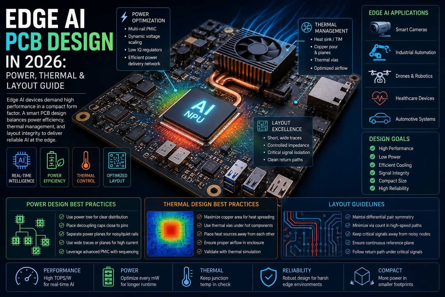
Edge AI PCB design in 2026 looks nothing like the low-power embedded layouts most teams cut their teeth on. Edge processors now hit tens of TOPS and run multi-billion-parameter models on-device, which means the inference workload that used to live in a server rack is now sitting on a board the size of a credit card. That shift changes most layout decisions: power delivery, thermal pathways, signal integrity, and stackup.
This article covers the layout patterns that work under real edge AI workloads, where the most common failures occur, and the design practices we see in production in 2026.
Key Takeaways
- Edge AI workloads draw 3–8 W sustained and peak above 15 W — power delivery and thermal design have to change accordingly.
- Plan for four to eight separate voltage rails, with point-of-load regulators within 10–15 mm of the SoC.
- Treat thermal as a first-order constraint at placement time, not a check you do at sign-off.
- LPDDR5 routing demands intra-byte skew under 50 ps and a continuous reference plane.
- BGA pitch ≤ 0.5 mm or more than four memory byte lanes means HDI from the start.
Why Edge AI Changes PCB Design
Traditional MCU-based embedded systems are bursty by nature. Wake up, sample a sensor, do a small computation, sleep. Power draw is measured in milliwatts. Thermal management is rarely a first-order concern.
Edge AI accelerators behave differently. A vision pipeline running continuous inference on a small neural network can draw 3–8 W sustained. Modern SoCs that combine a CPU, NPU, and ISP routinely peak above 15 W under load. That power has to be delivered cleanly to dozens of rails, and the heat it generates has to leave the package fast enough to keep junction temperatures within spec.
Traditional MCU vs Edge AI Workload Profile
| Design dimension | Traditional MCU board | Edge AI board (2026) |
|---|---|---|
| Sustained power | 10–500 mW | 3–8 W (15 W+ peak) |
| Voltage rails | 1–2 | 4–8 |
| Memory interface | SPI / I²C / parallel | LPDDR4 / LPDDR5 multi-Gbps |
| BGA pitch | 0.8 mm or larger | 0.4–0.5 mm common |
| Thermal strategy | Passive ambient | Vias + planes + active in some |
| Stackup | 2–4 layers | 6–10 layers, often HDI |
| Decoupling cap count | Tens | Often >100 |
The implication for PCB design for edge AI: a layout optimized for a low-power MCU will not survive a real edge AI workload. Power delivery, thermal management, and signal integrity all need to be reconsidered from first principles.
Power Delivery: From Single Rails to Multi-Phase Networks
Modern edge AI SoCs typically expose four to eight separate voltage rails — core, NPU, memory controller, IO, PHY, and analog domains. Each has its own ripple budget and transient response requirement.
Place Point-of-Load Regulators Close to the SoC
Long copper between a buck converter and the SoC creates inductance that crushes transient response. For NPU and memory rails, the regulator should sit within 10–15 mm of the package whenever the layout permits. The shorter trace is not a luxury — it is the difference between a stable rail under a load step and a brown-out during inference.
Use Multi-Phase Regulators for the Core Rail
Two-phase or four-phase converters spread the current across multiple inductors and capacitor banks. That reduces ripple and improves load-step response, which matters because NPU current draw can swing several amps in microseconds when an inference cycle starts. For sustained edge AI loads above 5 A, multi-phase is no longer optional.
Plan the Decoupling Capacitor Hierarchy
A typical edge AI rail benefits from a layered mix:
- A few hundred microfarads of bulk polymer near the regulator
- Multiple 10 µF MLCCs near the package
- 100 nF and 10 nF caps at every power pin
Decoupling capacitor performance is dominated by the loop inductance back to the ground plane, not the capacitor's ESR. Skipping the high-frequency caps is a common cause of inference failures that present as firmware bugs but trace back to the PDN.
Stitch Ground Planes Aggressively
Use a continuous ground reference under power planes. Stitch with vias frequently along high-current return paths. This improves EMI margin and signal integrity downstream at low cost.
Thermal Management: A First-Order Constraint
In 2026, thermal is no longer something you check at the end. It needs to be considered during component placement and stackup decisions, because the geometry of the heat path is locked in long before routing finishes.
Thermal Via Arrays Under the Package
The dominant heat path for most edge AI packages is downward through the board, then out via copper area, thermal vias, or a heatsink coupled to the back side. A grid of vias under the SoC's thermal pad, dropping into a large internal copper plane, is the cheapest and most effective way to spread heat. Aim for 0.3 mm via diameters at 1.0 mm pitch, plated through. Consider via-in-pad with epoxy fill if reflow voiding becomes a problem.
Increase Copper Weight on Inner Planes
Moving from 1 oz to 2 oz copper on power and ground layers improves both current handling and lateral heat spreading. For sustained loads above 5 W, the upgrade often pays for itself in reduced heatsinking requirements. Talk to your fab early — not every house holds the same thermal-via and heavy-copper capability at the same lead time.
Consider Metal-Core Substrates for Harsh Environments
Industrial and automotive edge AI applications benefit from MCPCBs or hybrid stackups that move heat off the board into a chassis. The cost premium is justifiable when ambient temperatures or enclosure constraints rule out conventional FR-4. Aerospace and outdoor sensor designs often fall into this bucket.
Run Thermal Simulation Early
A simple steady-state thermal sim during placement catches the layout-level mistakes that no amount of mechanical heatsinking can rescue. The gap between simulation and measured junction temperature on a well-modeled board is typically within a few degrees, which is enough margin to make placement decisions before routing.
LPDDR5 Routing and Signal Integrity for Edge AI PCBs
Edge AI SoCs almost always pair with LPDDR4 or LPDDR5 memory running at multi-gigabit data rates. These interfaces are sensitive to layout mistakes.
Length-Match Within Byte Lanes
LPDDR5 expects intra-byte skew under tight tolerances — typically under 50 ps at the BGA, which translates to roughly 3–5 mils depending on the substrate Dk. Use the design tool's net classes to match lane lengths to that tolerance. Route address and command signals together to maintain a consistent timing relationship.
Reference High-Speed Signals to a Continuous Plane
Crossing a plane split is one of the most common causes of failed memory eye diagrams. If a high-speed signal has to cross a split, place a stitching capacitor near the crossing. For DDR fly-by topologies, pay close attention to the termination network and the way the reference plane shifts under each device.
Watch Impedance on PCIe and High-Speed Serial
If the design includes PCIe Gen3 or Gen4 to a coprocessor, controlled impedance routing is mandatory. Specify the differential impedance to the fab, validate with TDR if possible, and use teardrops sparingly. The fab's stackup recommendation should drive your trace geometry, not the other way around.
Stackup Choices: When to Move to HDI
For edge AI designs that combine a high-pin-count BGA, multi-rail power delivery, and high-speed memory, conventional through-hole vias on a four- or six-layer stackup quickly run out of room.
HDI techniques — microvias, blind and buried vias, stacked or staggered via structures — give back the routing channels needed to escape a fine-pitch BGA cleanly. The cost premium for HDI has come down meaningfully as more fabs have added capability, and ultra-HDI with sub-25-micron traces is now available for designs that need it.
A practical guideline: if BGA pitch is 0.5 mm or finer, or if the design has more than four memory byte lanes, plan for HDI from the start. Retrofitting HDI to a layout that assumed standard PTH technology rarely goes well, and trying to escape a 0.4 mm BGA without microvias is often impossible at any layer count.
Practical Implications for Hardware Teams
The shift to edge AI workloads changes how the team approaches design. A few things worth doing on your next program:
- Run thermal and power-delivery analysis during placement, not after routing. By the time the layout is routed, the geometry of the heat path and the position of the regulators are baked in.
- Treat the BOM as part of the design decision. The MLCC count and value mix on a power-dense edge AI board can easily double from a comparable MCU board, with supply chain and assembly cost implications that should be visible early.
- Design with 20–30% headroom on thermal and current budgets. Continuous inference workloads stress every analog-domain assumption — leakage, regulator efficiency curves, capacitor self-heating. The headroom pays for itself the first time a customer ships a model update that pushes utilization higher than expected.
- Engage your fab early on stackup and HDI capability. Material choice, copper weight, and microvia structure decisions are easier to make before the placement is locked.
- Build a thermal-stress test into bring-up. Run the workload at full duty cycle in your worst-case enclosure and measure junction temperature directly. Surprises here are cheaper to find on the prototype than the production run.
Common Questions About Edge AI PCB Design
What power range should I budget for an edge AI board?
For a typical edge AI vision pipeline, plan for 3–8 W sustained at the SoC, with peaks of 15 W or more on heterogeneous packages that combine a CPU, NPU, and ISP. Add separate budgets for memory, sensors, connectivity, and any auxiliary accelerators on the board.
How many layers does an edge AI PCB need?
Six layers is a practical minimum for a single-SoC design with LPDDR5 memory. Designs with multiple memory channels, PCIe links, or two accelerators commonly land at eight to ten layers, often with HDI microvias for fine-pitch BGA escape.
Do I need HDI for every edge AI design?
No. HDI becomes mandatory when BGA pitch drops to 0.5 mm or finer, or when memory byte-lane density makes through-hole via escape impossible. For larger-pitch packages and lower memory channel counts, a well-routed conventional six-layer board can be enough.
What thermal management is required for an edge AI accelerator?
At minimum, a thermal-via array under the SoC's thermal pad dropping into a large internal copper plane. For sustained loads above 5 W, increase inner-plane copper weight to 2 oz. For loads above 10 W or harsh-environment designs, add a heatsink, MCPCB substrate, or active cooling.
What memory routing tolerances does LPDDR5 require?
LPDDR5 requires intra-byte skew below approximately 50 ps at the BGA, which translates to 3–5 mils depending on substrate Dk. Address and command signals should be routed together with a consistent reference plane, and any crossing of a plane split needs a stitching capacitor.
Working With Rapid Circuitry on Edge AI Boards
Edge AI puts new pressure on every layout. Power delivery, thermal management, signal integrity, and stackup choices that used to be optional optimizations are now baseline requirements. Teams that bring those constraints in early — at placement, not at sign-off — ship products that hold up under real workloads.
If you're working on an edge AI design and want a manufacturing partner that has built boards across these constraints, get in touch with Rapid Circuitry about your next prototype. We work on fine-pitch HDI, heavy-copper thermal stackups, and LPDDR5 routing regularly, and we're happy to flag the layout-level decisions that save a respin.
Need help with edge computing & ai hardware?
Get a free consultation with our expert engineers. We respond within 24 hours.
Get a Free ConsultationStay in the Loop
Subscribe to our newsletter for the latest updates and insights.
By subscribing, you agree to our Privacy Policy. You can unsubscribe at any time.