Single Pair Ethernet PCB Design 2026: 10BASE-T1S Guide
Single Pair Ethernet PCB design is becoming the default wiring strategy for industrial sensor and actuator networks in 2026, replacing decades of CAN, RS-485, and proprietary fieldbus runs. The driving standard, 10BASE-T1S (IEEE 802.3cg), brings IP-native 10 Mb/s communication down to the device level over a single unshielded twisted pair with optional bus power. For hardware teams, the transition changes how schematics, stackups, and topologies are laid out.
Key Takeaways
- Single Pair Ethernet PCB design centers on IEEE 802.3cg, with 10BASE-T1S supporting up to at least eight nodes on a 25 m mixing segment.
- Physical Layer Collision Avoidance (PLCA) replaces classical CSMA/CD so engineers must plan node IDs, TO_TIMER values, and BEACON timing in firmware.
- Layout discipline matters: short stubs (≤10 cm), tight differential pair geometry, and clean return paths protect signal integrity on the shared bus.
- Power over Data Lines (PoDL) per IEEE 802.3bu and the SPoE classes in 802.3cg let designers carry data and power on the same pair.
- Replacing CAN and RS-485 with 10BASE-T1S removes gateways, simplifies BOMs, and lets brownfield plants speak native TCP/IP across the edge.
Why Single Pair Ethernet PCB Design Matters for Industrial IoT in 2026
The push toward Single Pair Ethernet PCB design is being driven by a clear pain point. Industrial controls have lived on a patchwork of CAN, RS-485, Modbus, HART, and various proprietary fieldbuses for decades, with gateways doing the translation up to plant-level Ethernet. Each gateway adds latency, a single point of failure, and another firmware stack to maintain. 10BASE-T1S removes those translation layers by extending standard IEEE Ethernet down to the smallest sensor, and Single Pair Ethernet PCB design becomes the discipline that makes that extension reliable.
Three changes have made this realistic in 2026. Silicon options have multiplied, with NXP's TJA1410 and TJF1410 10BASE-T1S transceivers, Microchip's LAN867x and LAN865x 10BASE-T1S families, and Analog Devices' ADIN1100 and ADIN1110 for the longer-reach 10BASE-T1L. Reference designs from Arrow, Microchip, Bourns, and Amphenol now ship as evaluation kits aimed at brownfield migration. And industry groups like the OPEN Alliance and IEC SC65C have stabilized the connector, cable, and test specifications that integrators need to commit to a topology.
Where SPE Fits in the Stack
For most industrial deployments the picture looks like this. 10BASE-T1S handles the short multidrop runs between a controller and a cluster of sensors or actuators inside a machine. 10BASE-T1L handles the longer point-to-point runs back to a zonal switch or PLC, with reach up to 1,000 m as defined in IEEE 802.3cg. Above that, conventional 100BASE-TX and 1000BASE-T continue to handle backbone traffic. A Single Pair Ethernet PCB design does not try to replace gigabit links; it replaces the low-bandwidth, hard-to-extend buses that sit below them.
10BASE-T1S and PLCA: Physical Layer Fundamentals
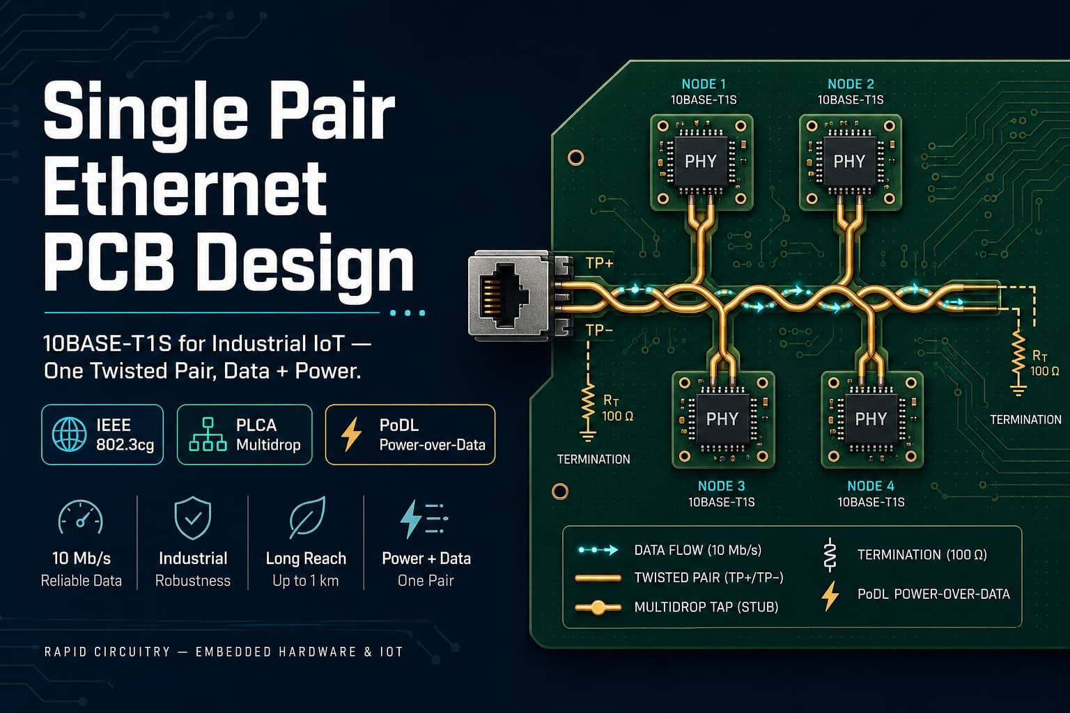
Before committing a Single Pair Ethernet PCB design to fab, the team should understand what the silicon expects from the board. 10BASE-T1S uses differential Manchester encoding at a 12.5 MBd symbol rate, with a nominal differential impedance of 100 Ω. The line is unshielded twisted pair, and IEEE 802.3cg allows half-duplex multidrop operation with up to at least eight in-line PHYs on a mixing segment of up to at least 25 m, with stubs of up to 10 cm at each tap.
What PLCA Changes
The hardest mental shift is collision handling. Classical Ethernet relies on CSMA/CD; on a short bus with eight devices, collisions and exponential backoff would crush throughput. PLCA (Physical Layer Collision Avoidance, defined in IEEE 802.3cg Clause 148) sidesteps the problem by giving each PHY a deterministic transmit opportunity in a round-robin cycle. A PLCA coordinator periodically emits a BEACON, then each node with PLCA ID 0, 1, 2 … in turn gets a TO (transmit opportunity) slot. If a node has nothing to send, it yields quickly and the next ID takes its turn.
Three PLCA parameters end up on every project's review checklist:
- plcanodecount: the upper bound on participating IDs. Set this to the maximum population the segment will ever see, not just the current node count.
- plca_id: must be unique per node on the segment, with the coordinator at ID 0.
- plcaburstcount and plcabursttimer: control how many back-to-back frames a node may send inside its slot, useful for tuning real-time control loops.
Why This Matters for PCB Designers
PLCA is firmware-configurable, but the board has to give the PHY clean, predictable signaling so the timing budget closes. That is where Single Pair Ethernet PCB design earns its keep.
Single Pair Ethernet PCB Design: Stackup, Routing, and Termination
Most 10BASE-T1S front ends look similar across vendors: a PHY with two differential pins (TRXP, TRXN), a small common-mode choke, a pair of DC-blocking capacitors, an ESD/EOS protection device, and a connector that meets the IEC 63171-x mating profile. The Single Pair Ethernet PCB design job is to get the differential pair from PHY to connector without disturbing the impedance or coupling noise into the shared bus.
A practical SPE board layout follows a few rules that show up on every project.
Stackup and Reference Planes
A four-layer stackup with signal–ground–power–signal is enough for most SPE nodes. Route the differential pair on an outer layer with a continuous ground reference directly beneath it. Avoid splitting the reference plane under the pair, and do not route the pair across a gap in the power plane on the layer below the reference. Discontinuities show up as common-mode noise on a bus that the PLCA timing budget assumes is clean.
Differential Pair Geometry
Target 100 Ω differential impedance with a tolerance of ±10 Ω, in line with Microchip's published LAN867x layout guide. Use matched length within roughly 5 mil, route the pair tightly coupled, and minimize via count between the PHY and the connector. If a via is unavoidable, place ground stitching vias within a few millimeters of each signal via on both sides of the plane transition.
Termination, Choke, and Caps
A 100 Ω AC termination across the pair near the connector controls reflections on the mixing segment. The common-mode choke sits between the PHY and the DC-blocking capacitors; pick a part rated for the PoDL current the node will draw, not just the data rate. DC-blocking capacitors are typically 100 nF, X7R, sized for the working voltage of the PoDL class in use.
Comparison: Wiring Options for Industrial Edge Nodes
| Property | RS-485 | CAN (Classic) | CAN FD | 10BASE-T1S | 10BASE-T1L |
|---|---|---|---|---|---|
| Data rate | 100 kb/s typical, up to 10 Mb/s short | 1 Mb/s | 5–8 Mb/s | 10 Mb/s | 10 Mb/s |
| Topology | Multidrop bus | Multidrop bus | Multidrop bus | Multidrop bus (PLCA) | Point-to-point |
| Max nodes (typical) | 32 (transceiver dependent) | 110 (transceiver dependent) | 110 | At least 8 per segment | 2 |
| Max length | 1,200 m at low rates | 40 m at 1 Mb/s | 5–10 m at 5 Mb/s | 25 m mixing segment | 1,000 m |
| Native IP | No | No | No | Yes | Yes |
| Power on pair | No (separate) | No (separate) | No (separate) | PoDL (802.3bu/cg) | PoDL/SPoE |
| Standards body | TIA/EIA | ISO 11898 | ISO 11898-1 | IEEE 802.3cg | IEEE 802.3cg |
The cable-length numbers come from each protocol's standard rather than vendor marketing, and they are the practical limits a hardware team should plan around when sizing a zone.
Multidrop Topology in Single Pair Ethernet PCB Design
Single Pair Ethernet PCB design extends beyond a single board. On a 10BASE-T1S mixing segment, each node is a stub on the shared bus, and every connector, T-junction, and trace length contributes to the signal picture seen by every other PHY.
Stub Length Discipline
IEEE 802.3cg sets 10 cm as the maximum stub length from the bus to any PHY. That budget includes the cable from the inline connector to the PCB, plus the trace on the PCB from the connector to the PHY's differential pins. Hardware teams that put the PHY 5 cm from the connector with a 6 cm pigtail will be over budget before they ship. Plan the enclosure and connector placement in any Single Pair Ethernet PCB design around the stub limit, not the other way around.
Termination Strategy
The two end nodes on the segment terminate the line. Intermediate nodes are tap points and do not terminate. Baking a termination into every node, common in CAN habits, absorbs signal energy and degrades timing margins. Make the termination either DIP-switch selectable or a populated/depopulated 0 Ω jumper, so the same PCB can serve as an end node or a mid-bus tap.
Cabling and Connectors
The connector ecosystem has consolidated around IEC 63171-6 (the T1 industrial style popularized by HARTING and Phoenix Contact, with M8 hybrid variants for harsh-environment use) and IEC 63171-1 (the LC-Style developed by CommScope, Panduit, and Reichle for office and light-industrial use). Cable picks usually follow the ISO/IEC 11801-1 SPE link classes, with unshielded twisted-pair acceptable in benign environments and shielded variants recommended near variable-frequency drives or welding equipment. Document the chosen connector and cable class in the assembly drawing so installers do not improvise in the field.
Power over Data Lines (PoDL) in Single Pair Ethernet PCB Design
One of the bigger savings from a Single Pair Ethernet PCB design is removing the second cable that traditionally carried power to a sensor. IEEE 802.3bu defined the original PoDL profile for 100BASE-T1 and 1000BASE-T1, and the 802.3cg amendment introduced SPoE classes that align with the 10BASE-T1S and 10BASE-T1L use cases. Per IEEE 802.3cg and the Ethernet Alliance SPoE tech brief, practical SPoE classes range from sub-watt at 24 V for low-power sensors up to roughly 50 W at 55 V for actuators on short, well-conditioned cabling.
What This Means on the Board
PoDL needs a PSE (Power Sourcing Equipment) controller on the powered-trunk side and a PD (Powered Device) controller on the node. On the node PCB in a PoDL-capable Single Pair Ethernet PCB design, route the bias-tee components (inductors that pass DC but block the AC signal, plus the DC-blocking caps already in the data path) close to the connector. Keep the bias inductors well away from the differential pair, and ground their cans cleanly. Size the bulk capacitance after the PD controller for the inrush behavior the spec requires.
Safety and Isolation
Industrial SPoE classes can push 55 V on the cable. Treat the PoDL rail as any low-voltage industrial DC bus: respect creepage and clearance per IPC-2221B or IEC 60664-1, fuse the input, and provide reverse-polarity protection. If the node connects to a mains-driven motor controller elsewhere on the machine, plan the isolation barrier into the schematic up front, not as a late ECO.
Practical Implications for Hardware Teams
The transition to Single Pair Ethernet PCB design is rarely a single-board exercise. It usually touches the whole product family.
- Treat the first Single Pair Ethernet PCB design as a platform decision. The PHY, connector, ESD device, and PoDL controller will repeat across every sensor and actuator in the line.
- Build a PLCA configuration table early and version-control it like any interface contract.
- Add SPE bus traffic capture to the test plan. Commercial 10BASE-T1S analyzers remove a lot of guesswork during bring-up.
- Pilot a mixed-vendor segment before locking in a single silicon supplier. PLCA interoperability has improved, but timing edge cases still surface.
- Document the segment topology, stub lengths, termination locations, and PLCA IDs in the released drawing set. Field engineers will need that map when a sensor is added two years later.
Common Questions About Single Pair Ethernet PCB Design
What is Single Pair Ethernet?
Single Pair Ethernet is a family of IEEE 802.3 physical layers that carry Ethernet over a single twisted pair instead of the two or four pairs used by 100BASE-TX or 1000BASE-T. The variants most relevant to industrial IoT are 10BASE-T1S (multidrop, short reach) and 10BASE-T1L (point-to-point, up to 1,000 m), both in IEEE 802.3cg.
How is 10BASE-T1S different from 10BASE-T?
10BASE-T runs at 10 Mb/s over two pairs of Cat. 3 or better cable in a star topology. 10BASE-T1S runs at the same 10 Mb/s but on a single twisted pair, supports a multidrop bus with at least eight nodes on a 25 m segment, and uses PLCA instead of CSMA/CD. The PHY, connector, and cabling are not interchangeable.
What is PLCA and why is it needed?
PLCA, or Physical Layer Collision Avoidance, is defined in IEEE 802.3cg Clause 148. It gives each node on a 10BASE-T1S bus a deterministic transmit opportunity in a round-robin cycle initiated by a BEACON from the coordinator. PLCA avoids the collision-and-backoff behavior of CSMA/CD, which would otherwise dominate latency on a short multidrop segment.
How long can a 10BASE-T1S mixing segment be?
The standard specifies at least 25 m of mixing segment with up to at least eight in-line PHYs and stub lengths up to 10 cm at each tap. Many implementations achieve more than the minimum, but designs should plan to the standard's guaranteed numbers and validate any margin in the lab.
Does 10BASE-T1S support Power over Data Lines?
Yes. The 802.3cg amendment defines SPoE classes that build on IEEE 802.3bu PoDL, letting the same pair carry data and DC power. Available power ranges from a few hundred milliwatts to roughly 50 W depending on the class, the cable, and the segment topology.
Can you replace CAN or RS-485 with 10BASE-T1S?
In most new industrial designs, yes. 10BASE-T1S brings native TCP/IP, deterministic media access through PLCA, headroom for firmware updates and diagnostics, and the option of PoDL on the same pair. Existing CAN deployments rarely justify a forklift upgrade, but new platforms can skip the gateway and run Ethernet end to end.
Working With Rapid Circuitry on Single Pair Ethernet Designs
Single Pair Ethernet PCB design is straightforward once a team has done it twice, and painful the first time, when stub budgets, termination strategy, and PLCA timing all show up at once. We work with hardware groups on the parts that matter early: PHY and PoDL selection, stackup definition, the first multidrop interoperability sweep, and the test fixtures that make field bring-up predictable. If you are planning a sensor or actuator family that will retire a CAN or RS-485 backbone, or migrating a brownfield line to zonal Ethernet, we are happy to look at the schematic. You can reach us through our PCB design service page, our embedded hardware engineering team, or the industrial automation practice for the system-level view. For deeper protocol references, the IEEE 802.3cg standard, Microchip's 10BASE-T1S layout guide, and the OPEN Alliance 10BASE-T1S system implementation specification are the documents we keep open while we work.
Need help with industrial iot (iiot) & automation?
Get a free consultation with our expert engineers. We respond within 24 hours.
Get a Free ConsultationStay in the Loop
Subscribe to our newsletter for the latest updates and insights.
By subscribing, you agree to our Privacy Policy. You can unsubscribe at any time.