GaN Bidirectional Switches 2026: PCB Layout & Topology Guide
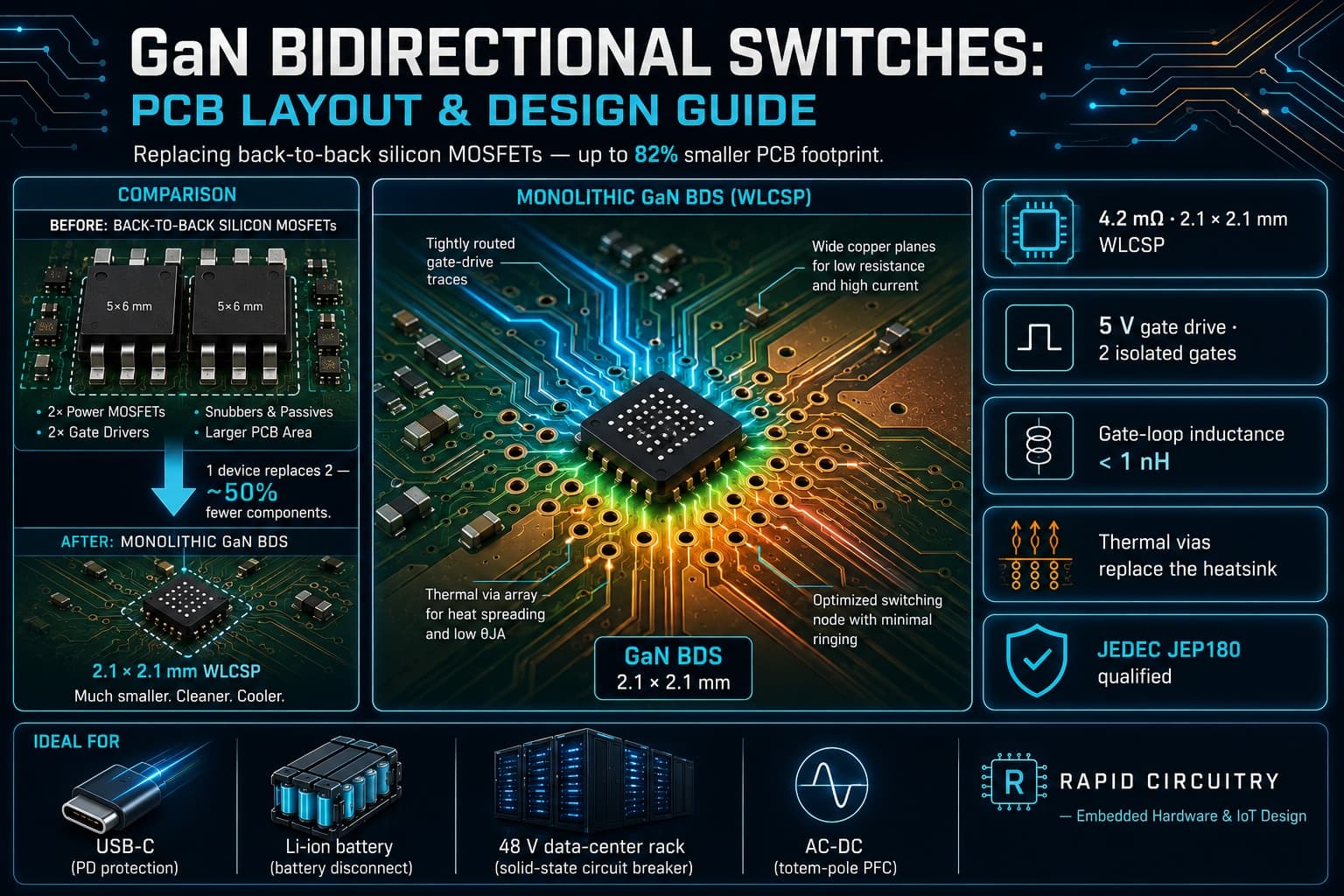
GaN bidirectional switches are replacing the back-to-back silicon MOSFET pair that handled four-quadrant switching in chargers, USB protection, and battery disconnects for two decades. With Infineon's May 2026 expansion of the CoolGaN BDS 40 V G3 family delivering up to 82 percent PCB footprint reduction in 2.1 x 2.1 mm WLCSP, the conversation has shifted from "is this technology ready" to "how do I lay out GaN bidirectional switches without losing the gains."
Key Takeaways
- A monolithic GaN bidirectional switch replaces two discrete MOSFETs and their gate-drive network with a single device, cutting component count by roughly 50 percent.
- WLCSP GaN BDS packages reach sub-2 mm pitch, which moves the dominant layout constraint from device size to via inductance and copper spreading.
- Common-source-pair operation requires two independently driven, isolated gates with low loop inductance; layout discipline matters more than absolute trace width.
- A 5 V gate drive simplifies the bill of materials but tightens the noise budget for the gate return path.
- Thermal performance in a 2 x 2 mm WLCSP is dominated by copper area under the pads, board thickness, and the bottom-side return path; thermal vias replace the heatsink.
- Reliability qualification still tracks JEDEC JEP180 for GaN power devices, so the PCB layout has to support the dynamic R(DS,on) and short-circuit behavior the part was qualified against.
What GaN Bidirectional Switches Replace on a Power PCB
A GaN bidirectional switch is a single die that can block voltage and conduct current in both polarities. The traditional silicon answer was two MOSFETs source-to-source or drain-to-drain, with one isolated gate driver per FET plus snubbers, bootstraps, and the layout area to keep them clean.
A monolithic GaN bidirectional switch collapses that to one part. Infineon's CoolGaN BDS 40 V G3 release places the IGK048B041S (4.2 mOhm) in a 2.1 x 2.1 mm package and the IGK120B041S (9 mOhm) in a 1.7 x 1.2 mm package, both with 5 V gate drive. The topology cuts component count in half and shrinks PCB footprint by up to 82 percent in portable power designs.
Where Bidirectional Switching Actually Matters
The function is essential where the load can source or sink current, or where the protected line can swing polarity. Common applications include USB Type-C and USB PD overvoltage and reverse-polarity protection on smartphones and notebooks, battery disconnect for multi-cell Li-ion packs (charge and discharge currents each blockable independently), solid-state circuit breakers in 48 V data center distribution that must clear faults in either direction, and single-stage AC-DC topologies such as totem-pole PFC variants and matrix converters that need true four-quadrant operation.
In each case the conventional answer is a back-to-back MOSFET pair. A monolithic GaN bidirectional switch removes most of that footprint without changing the system function.
Topology Choices for GaN Bidirectional Switches: Monolithic vs Discrete
Not every bidirectional design wants a monolithic part. The trade is package thermal capacity and gate-drive complexity against component count and board area. The decision turns on power level, switching frequency, and how aggressive the form factor needs to be.
Monolithic GaN BDS
A monolithic GaN bidirectional switch has two isolated gate terminals and one shared drift region. Each gate controls one direction of conduction. To turn the switch fully on, both gates are driven; to block in either direction, the corresponding gate is held off. The shared drift region is what gives the package its area advantage, because there is only one channel to spread heat from.
The cost is that gate-drive timing matters more than with discrete pairs. Short gate skew can put both gates in transition simultaneously, which the part tolerates but which costs efficiency every cycle. Datasheets specify recommended gate-drive sequencing; the layout must support the timing the driver promises.
Discrete Common-Source Pair
The discrete approach uses two enhancement-mode GaN HEMTs (or silicon MOSFETs at lower frequencies) connected source-to-source, with the shared source node tied to the gate-driver ground reference. A single isolated gate driver can then control both gates simultaneously, with one device's third-quadrant conduction handling the off-state path.
Discrete pairs win when the design needs more thermal headroom than a 2 x 2 mm WLCSP can deliver, or when the application already has isolated gate drivers on the BOM. They lose on board area, gate-loop inductance, and parts cost above roughly 10 W of continuous dissipation.
Comparison Table
| Criterion | Monolithic GaN BDS (e.g., CoolGaN BDS 40 V G3) | Discrete Common-Source eGaN Pair | Back-to-Back Silicon MOSFETs |
|---|---|---|---|
| Typical package | WLCSP 1.7 x 1.2 mm to 2.1 x 2.1 mm | Two PQFN 3 x 3 mm | Two PQFN 5 x 6 mm |
| Gate drives required | 2 (one per gate, shared source) | 1 isolated (shared gate) | 2 isolated |
| Continuous current at 25 C | Up to ~12 A in current 40 V parts | 15 to 30 A per FET | 20 to 60 A per FET |
| Footprint vs silicon pair | Up to ~82% smaller | ~40-60% smaller | Baseline |
| Best fit | Portable power, USB protection, wearables | 100 W class chargers, 48 V SSCBs | Legacy, high-current, low-cost |
| Thermal handling | Board-limited; relies on copper spreading | Package-limited; tab plus airflow | Package-limited; through-hole heatsink common |
PCB Layout Rules for GaN Bidirectional Switches
The two practical risks at layout time are gate-loop inductance and switching-node copper area. GaN switches at hundreds of volts per nanosecond. Any inductance in series with the gate delays turn-on or causes overshoot at turn-off; inductance in the power loop becomes a voltage spike that eats into the safe operating area.
Gate Loop Discipline
A 5 V gate drive gives a tight noise budget. The Miller plateau on a GaN HEMT sits near 2 V, so a 1 V transient from a poorly placed decoupling cap can re-trigger a switching event. Three rules cover most of the gate-loop work:
- Place the gate-drive decoupling capacitor on the same side of the board as the driver, within 5 mm of the VCC pin, with the ground via inside the cap footprint when DFM allows.
- Route the gate trace and its return as a tightly coupled pair, on adjacent layers with the gate return as a continuous reference plane under the trace.
- Bring the source kelvin connection (where the package provides one) back to the gate-driver ground separately from the high-current source path. On a WLCSP without a dedicated kelvin pad, treat the bottom-side ground via array as the kelvin reference.
Switching Node and Power Loop
The switching node sits between the two channels of the bidirectional switch. It carries the full load current and switches at high dV/dt, so it is both a heat source and a radiator. Keep its copper area as small as electrical performance allows — parasitic capacitance to ground on the switching node feeds dV/dt current into the wrong place.
The power loop, from bus capacitor through the switch and back, should sit on adjacent layers separated only by the dielectric. Loop inductance below 1 nH is achievable on a 4-layer board with 8-mil dielectric and disciplined via placement. Above 2 nH, the voltage overshoot at typical switching speeds eats the headroom on a 40 V part.
Decoupling and Return Paths
For a 40 V GaN bidirectional switch, two ceramic capacitors per device handle the bypass: a 100 nF X7R close to the bus pin and a 1 uF X7R one footprint away, both with via-in-pad or pad-side vias. The ground side belongs on the same plane that carries the source return, with no plane splits between the cap and the device.
IPC-2221 sets the baseline trace and clearance rules, but at GaN switching speeds the limiting factor on a supply trace is inductance per unit length, not current-carrying capacity. A 1 mm-wide trace 5 mm long is roughly 3 nH; the same path as a plane pour is roughly 0.3 nH. Use plane pours for everything that switches.
Thermal Management for GaN Bidirectional Switches
A 2 x 2 mm WLCSP cannot dissipate 2 W on its own. The board does the work. The thermal design of a GaN bidirectional switch PCB is the thermal design of the copper under and around the part.
Copper Spreading and Thermal Vias
The first 5 mm of copper outward from the device pads carries the steepest temperature gradient and the most useful spreading. Plane pours on both sides of the board, joined by a thermal via array under the device, are the standard pattern. A typical layout uses 0.3 mm vias on a 0.5 mm grid, with via-in-pad on the highest-current balls.
IPC-2152 gives the baseline curves for current-carrying capacity as a function of copper weight and area; the same curves are the starting point for thermal sizing of a power pad. For a GaN bidirectional switch dissipating 1 W in a 2 x 2 mm package on 1 oz outer copper, expect a junction-to-ambient rise of roughly 60 to 80 C without forced air, dropping to 30 to 45 C with modest airflow and 1 cm2 of pour.
Board Stackup for Power
A 4-layer board with 1 oz outer and 1 oz inner copper is the practical minimum above 5 W of dissipation. 2 oz inner copper roughly halves spreading resistance and is usually cheaper than adding airflow. For consumer products with no fan budget, 6 layers with ground planes on layers 2 and 5 doubles lateral spreading without changing board thickness.
Reliability and Qualification
GaN HEMTs have a dynamic R(DS,on) behavior that depends on switching history; the device qualified for an application has been tested against a specific switching profile, and the PCB layout has to keep the part inside that profile. JEDEC JEP180 is the industry guideline for GaN power device reliability qualification and the reference most vendors cite in their datasheets. If a layout pushes the part outside that envelope — higher dV/dt than tested, harsher thermal cycling, or operation outside the gate-drive recommendations — the field reliability data the vendor publishes no longer applies.
Practical Implications for Hardware Teams
- Audit any new portable power, USB protection, or battery-disconnect design for a monolithic GaN bidirectional switch swap. The component-count saving alone often pays for the redesign within one production run.
- Budget gate-drive selection alongside the BDS choice. Two-channel isolated drivers with matched propagation delay (within a few nanoseconds) set the practical floor on switching-node cleanness.
- Plan the layout for 5 V gate logic. Mixing a 12 V silicon-FET driver topology into a GaN bidirectional switch schematic is a common cause of overshoot and gate damage in pilot builds.
- Treat the WLCSP land pattern as a thermal pad, not a footprint. Plan copper area, thermal via grid, and stackup before pin assignment is finalized; reworking copper after routing is twice the effort.
- Confirm JEDEC JEP180 qualification status on any GaN bidirectional switch before it lands in a production BOM. Engineering samples often predate full qualification.
- Push pre-compliance EMI scans earlier in the schedule. GaN switching edges put more energy above 100 MHz than a silicon equivalent, and filter rework after EVT is expensive.
Common Questions About GaN Bidirectional Switches
What is a GaN bidirectional switch?
A GaN bidirectional switch is a single semiconductor device that can block voltage and conduct current in both polarities, replacing a back-to-back pair of MOSFETs. Monolithic versions use one drift region with two isolated gates, while discrete implementations use two enhancement-mode GaN HEMTs in a common-source pair.
When is a monolithic GaN BDS better than two back-to-back MOSFETs?
Below roughly 10 W of continuous dissipation and where board area is constrained, the monolithic part wins on size, parts count, and gate-loop inductance. Above 10 W, or in designs that already carry isolated gate drivers for other rails, a discrete pair gives more thermal margin and supply flexibility.
How small can a GaN bidirectional switch get?
Current production parts reach 1.7 x 1.2 mm WLCSP at 9 mOhm and 2.1 x 2.1 mm WLCSP at 4.2 mOhm in the 40 V class. The package size floor is set by the minimum copper area needed to dissipate the part's continuous power, not by the die itself; smaller dies exist but cannot run at rated current in a sub-2 mm package without active cooling.
Do GaN bidirectional switches need special gate drivers?
Yes. Two independent channels are required, each with its own ground reference at the device source. The 5 V gate drive used on modern BDS parts requires a driver with a tight Miller-plateau crossing time and matched propagation delay between channels. Many silicon-FET drivers are not suitable without external level translation.
What thermal pad design do GaN BDS WLCSP packages need?
A continuous copper pour of at least 1 cm2 connected to the source and drain balls on both sides of the board, joined by a thermal via array (typically 0.3 mm vias on a 0.5 mm grid), is the conventional starting point. The 1 oz outer copper baseline assumed by IPC-2152 is the floor; 2 oz inner copper helps spread heat away from the device under sustained dissipation.
Are GaN bidirectional switches qualified for automotive use?
The 40 V consumer parts shipping today are qualified for consumer and industrial applications. Automotive-grade GaN BDS (AEC-Q101 plus PPAP-ready material declarations) is an active product line for most vendors but not yet broadly catalogued. Teams targeting connected-vehicle hardware should request qualification status in writing before committing a BDS to a production BOM.
Working With Rapid Circuitry on GaN Power Designs
A GaN bidirectional switch on the BOM changes the layout work, the EMI test plan, and the thermal model. The component is small; the engineering around it is not. Our PCB design team handles the gate-loop discipline, thermal spreading, and pre-compliance work that decides whether a BDS design hits the same yield as the silicon design it replaced. Our electronics design service takes a BDS from datasheet to qualified hardware, with pre-compliance EMI captured in-house before formal compliance testing. If you are evaluating a GaN bidirectional switch for an upcoming product, get in touch and we will scope the layout and qualification path against your form factor and timeline.
Need help with power electronics & energy harvesting?
Get a free consultation with our expert engineers. We respond within 24 hours.
Get a Free ConsultationStay in the Loop
Subscribe to our newsletter for the latest updates and insights.
By subscribing, you agree to our Privacy Policy. You can unsubscribe at any time.